Photonic-crystal surface-emitting lasers

Introduction
Lasers, together with digital technologies including digital twins and machine learning, could become indispensable components of smart mobility1 and smart manufacturing2. By virtue of many performance advantages including small sizes, low cost and high efficiency, semiconductor lasers are considered one of the most promising laser technologies for these emerging applications. However, conventional semiconductor lasers, including edge-emitting lasers and vertical-cavity surface-emitting lasers3,4,5,6, are inherently incapable of achieving functionalities such as on-chip beam scanning and generation of arbitrarily shaped beams. They also have insufficient brightness (≤100 MW cm−2 sr−1), which is defined as the optical power per unit area per unit solid angle and expresses how narrowly a laser beam diverges or how intensely a laser beam can be focused. Therefore, for application in smart mobility of robotics and vehicles, conventional semiconductor lasers require complicated lens systems and fine adjustments to reshape and collimate the emitted beams. In addition, the emitted beams are usually scanned mechanically by using external mirrors and motors, making the systems larger and more complicated. Furthermore, for smart manufacturing applications, the low brightness of semiconductor lasers hinders their direct applications in laser processing. Instead, one must rely on gas and solid-state lasers (including fibre lasers), which are very large and complicated and have low efficiencies. Therefore, a new laser technology that can address the above issues, by being compact, yet capable of high-brightness and high-functionality operation, is urgently needed.
Photonic-crystal surface-emitting lasers (PCSELs)7,8,9,10,11,12,13,14,15,16,17,18,19,20,21,22,23,24,25,26,27,28 are a new type of laser that possesses high brightness as well as high functionalities (such as on-chip beam scanning and generation of any beam pattern), while also maintaining the merits of semiconductor lasers. PCSELs are based on the formation of large-area two-dimensional (2D) standing-wave resonances through optical diffraction (or mutual coupling) of light waves propagating inside a 2D photonic crystal, enabling high-power, high-beam-quality operation. This oscillation corresponds to the use of singularity points (Γ2, M1 and so on) where the group velocity of light becomes zero, in optical dispersion relations known as the photonic band structure (see next section for details)7,11,17. Although research on PCSELs started in the late 1990s7,8, it is the most recent work that has improved their brightness16,18,19. In particular, a brightness of 1 GW cm−2 sr−1, comparable to that of existing bulky lasers, has been realized under pulsed conditions29 and even under continuous-wave (CW) conditions20. In addition, various functionalities, such as electronic 2D beam scanning17,21 and the generation of arbitrarily shaped beams17,21,22, have been achieved with PCSELs.
Further notable developments of PCSELs include short-pulse (<100 ps) and high-peak-power (>100 W) operation23,24, as well as short-wavelength (~430 nm) operation25. The former has been realized by introducing advanced Q-switching mechanisms, and the latter by expanding the material system to wide-bandgap GaN, both of which will be described in later sections. Furthermore, efforts towards the integration of PCSELs with machine learning and quantum computing26,27 are underway.
In this Review, we describe the recent progress in high-brightness and high-functionality operations of PCSELs as well as new research trends. We also elaborate on recent developments relative to the applications of PCSELs for smart mobility and smart manufacturing, as well as broader implementations of PCSELs in smart society. Finally, we summarize future research directions in the fields such as aerospace and laser fusion and outline the remaining challenges toward achieving the required brightness and power for such fields.
Basic lasing principle of PCSELs
A typical structure of a PCSEL consists of a photonic-crystal layer with a periodic refractive-index distribution (that is, periodically arranged air holes), an active layer for light amplification, and a pair of cladding layers and electrodes for current injection (Fig. 1a). For amplification in the active layer, interband transitions in quantum wells, which have optical gain with transverse-electric polarization, are commonly used in PCSELs, akin to conventional semiconductor lasers, whereas intersubband transitions in quantum wells, which have optical gain with transverse-magnetic polarization, can be used for quantum-cascade-based PCSELs13,30. Interband transitions of quantum dots can be also used for amplification in the active layer of PCSELs31. When the current is injected into the active layer through the cladding layers, light is generated within the active layer and is trapped between the active and cladding layers by total internal reflection while also being coupled to the photonic-crystal layer. Inside the photonic crystal, light waves propagating in several in-plane directions are coupled with each other, leading to 2D coherent lasing with surface emission.

a, Schematic of photonic-crystal surface-emitting lasers (PCSELs). b, Basic lasing principle of PCSELs. The left panel shows the schematic of optical diffractions of fundamental light waves (yellow arrows) and high-order light waves (blue arrows) inside the photonic crystal, where each air hole inside the photonic crystal works as a ‘mirror’ to induce in-plane 180° or 90° diffractions and as a ‘nanoantenna’ to induce out-of-plane diffraction into radiative waves (red arrows). Here, a is the lattice constant of the photonic crystal and λ is the wavelength of light measured inside the material. The right panel shows an example of an electromagnetic-field distribution of 2D coherent resonance with surface emission. Arrows denote in-plane electric-field vectors (Ex,Ey), and colour denotes the amplitude of the out-of-plane magnetic field vector (Hz). c, Typical photonic band structure of a 2D photonic crystal. The band edges are labelled A, B, C and D in order of increasing frequency. AR, anti-reflection; c, the speed of light in a vacuum.
The lasing mechanism of typical square-lattice PCSELs that emit light in the vertical direction is shown in Fig. 1b (leftmost panel), illustrating a schematic of a square-lattice photonic crystal, where the distance a between the two air holes (lattice constant) of the photonic crystal is set to be equal to the wavelength λ of light measured inside the material. In the photonic crystal layer, each air hole serves both as a ‘mirror’ to induce in-plane diffractions and as a ‘nanoantenna’ to induce out-of-plane diffractions. In other words, light waves propagating in the x and y directions (fundamental waves) are diffracted at each hole and change direction by 180° directly, and by 90° indirectly via other waves (that is, high-order waves propagating in different directions)32. In addition, the fundamental waves are also diffracted in the vertical direction as radiative waves (second panel from the left of Fig. 1b). Through these mutual in-plane and radiative diffractions inside the photonic crystal, a 2D standing-wave resonance is formed over a large area, and lasing oscillation accompanied by surface emission is obtained (Fig. 1b).
The above qualitative explanation can be described more rigorously. The diffractions induced by the periodic refractive-index distribution yield a photonic band structure, which has several singularity points such as Γ2 and M1 (Fig. 1c). At these singularity points, the group velocity of light becomes zero via the optical couplings among light waves propagating in various directions, resulting in the formation of 2D broad-area resonant modes. In the case when the lattice constant is equal to the wavelength measured inside the material, PCSELs operate at the Γ2 points (Fig. 1c) above the light line, where the total internal reflection of light does not occur, allowing direct surface emission. Conversely, when the lattice constant is equal to (1/sqrt{2}) of the wavelength, PCSELs operate at the M1 points (Fig. 1c) below the light line, where surface emission is forbidden by the total internal reflection of light. In this situation, when ‘modulated photonic crystals’ are introduced (as described in the section ‘High-functionality PCSELs’), advanced surface-emitting functionalities, such as 2D beam scanning and arbitrary beam-pattern generation, can be achieved.
One of the most important features of PCSELs is the capability of single-mode oscillation in an emission area that is many times wider than in conventional semiconductor lasers17,18,19,20,33. The first step toward enabling large-area single-mode lasing is to increase the threshold gain difference between the lasing band-edge mode and other band-edge modes at the same singularity point. For example, at each singularity point of a square-lattice photonic crystal, there exist modes on four different band edges A to D (Fig. 1c). As the modes of each of these band edges have different electric-field distributions inside the unit cell, only one of the four modes can be selected as a lasing mode, by manipulating the asymmetry of the unit-cell structure and the interference of radiation of each mode in the far field17,32,33. Also, when the device size becomes larger than several hundred micrometres in diameter, mode competition between fundamental and higher-order modes within the same band, where the electric-field intensity of the fundamental mode is highest at the centre of the device and that of the higher-order modes is highest near its edges, becomes an important consideration (Fig. 2c). For this purpose, the optical losses of the higher-order modes should be sufficiently higher than that of the fundamental mode, as described in the next section. Lasing states in such large-area PCSELs can be modelled by 3D coupled-wave theory19,32,34. For more comprehensive explanations on the lasing principle and numerical simulation of PCSELs, we refer the readers to previous work33.

a, Beam propagation characteristics without external lenses for a conventional semiconductor laser (a broad-area edge-emitting type) and a 500-µm-diameter photonic-crystal surface-emitting laser (PCSEL). The beam patterns are observed by placing a screen at various distances from the laser, then monitoring the screen with an infrared camera. Owing to the high brightness of the PCSEL, the divergence angle of the beam emitted is very narrow, and therefore the beam can be observed at a much greater distance than that of the conventional laser. b, A class-minimum mechanical light detection and ranging (LiDAR) system equipped with a 500-μm-diameter PCSEL. c, Electric-field intensity distribution of the fundamental mode (left) and a higher-order (first-order) mode (right) in a PCSEL. d, Schematic of radiation of the fundamental mode (left) and higher-order (first-order) mode (right) in a PCSEL19,20. e, ‘Double-lattice’ photonic crystal, in which destructive interference for in-plane 180° diffraction and/or for both in-plane 180° and 90° diffractions are introduced (left)18,19,20 and in-plane 180° diffraction via radiative waves is additionally controlled (right)19,20. f, Calculated radiation loss as a function of in-plane wavenumber. Simultaneously reducing R and μ, where R is the real part of the coupling coefficient of combined in-plane 180° and 90° diffractions (Hermitian coupling) and μ is the 180° coupling coefficient through radiative waves (non-Hermitian coupling), increases the radiation loss at larger in-plane wavenumbers, corresponding to the higher-order modes19,20. Here, downward arrows indicate the in-plane wavenumbers of the fundamental and first higher-order modes, respectively, in a 3-mm-diameter PCSEL. For all combinations of R and μ, the imaginary part of Hermitian coupling, I, is adjusted to obtain an appropriate amount of radiation for the fundamental mode. g, Photograph of a 3-mm-diameter PCSEL. This PCSEL was mounted on a package for operation under continuous-wave (CW) conditions. h, I–L characteristics, lasing spectrum and far-field pattern (FFP) under CW conditions20. A narrow spectral width was observed. Single-mode lasing and a nearly diffraction-limited narrow beam were confirmed at a CW output power of 50 W. i, I–L characteristics and far-field pattern under pulsed conditions. The pulse width and repetition frequency were 50 ns and 100 Hz, respectively. j,k, Metal cutting (panel j) and colour marking (panel k) by a 3-mm-diameter high-brightness PCSEL. Panel a adapted from ref. 59, CC BY 4.0 (https://creativecommons.org/licenses/by/4.0/). Panels c,d,f and h reprinted from ref. 20, CC BY 4.0 (https://creativecommons.org/licenses/by/4.0/). Panel e adapted with permission from ref. 33, Optica Publishing Group. Panel k adapted with permission from ref. 36, Optica Publishing Group.
High-brightness PCSELs
For applications to smart mobility and smart manufacturing, high-brightness PCSELs operating at the Γ2 singularity point of the photonic crystal can be used, where collimated beams are emitted in the direction normal to the surface (Fig. 1a,b). Note that the applications for high-brightness PCSELs operating at the Γ2 singularity point are more diverse and include fields such as communications, mobile technology, medicine and aerospace.
For smart mobility of robots and vehicles, lasers are normally used for time-of-flight (ToF) light detection and ranging (LiDAR) in combination with detectors, where a light pulse is sent from a laser (or transmitter), and the reflected light from objects in the scene is then detected by a detector (or receiver). The obtained ToF signal is used to create a distance map of the objects in the scene. In this case, lasers operate under pulsed conditions, where electric current is injected for a few nanoseconds at intervals of a few microseconds. In such pulsed conditions, a PCSEL with a 500-μm diameter exhibits a very high brightness, above 1 GW cm−2 sr−1 (ref. 29), surpassing that of conventional semiconductor lasers by more than one order of magnitude. The beam of the conventional laser diverges significantly, whereas that of the PCSEL remains very narrow with a beam radius of only 5 cm even at 30 m (Fig. 2a). The key to realize such high-brightness operation is the use of a ‘double-lattice’ photonic crystal. A high-brightness PCSEL with a 500-μm diameter has been used to construct a class-minimum mechanical LiDAR system (Fig. 2b), where a complex lens system conventionally used to reshape and collimate the emitted beam is completely removed. This LiDAR system has even been applied to smart mobility of robots33,35. Moreover, high-throughput fabrication of 500-μm-diameter PCSELs based on nanoimprinting technologies has been demonstrated (Box 1), which, along with 1-year reliability tests, suggests commercialization potential of PCSELs.
To realize high-brightness operation of a 500-μm-diameter PCSEL, it is important to understand the fundamental and first higher-order modes of a PCSEL (Fig. 2c), as described in the previous section. When lasing oscillation occurs in higher-order modes, the beam quality deteriorates, leading to low-brightness operation. Thus, the loss of the higher-order modes must be selectively increased to suppress oscillation in these modes. A double-lattice structure, in which two square-lattice photonic crystals are overlapped with a separation (d) of around one-quarter of the wavelength of light in the device (panel a in the Box 1 figure and left panel of Fig. 2e), is key to this. At this separation, the optical path difference between light waves diffracted by the square lattice with the larger air holes and the one with the smaller air holes is approximately π, so destructive interference occurs mainly for in-plane 180° diffraction18, leading to in-plane spreading of the mode fields. Consequently, in-plane loss due to light escaping from the edge (Fig. 2c) of the resonator can be larger for higher-order modes than for the fundamental mode, because the antinodes of the higher-order modes are closer to the edge of the device. Thus, laser oscillation occurs in the fundamental mode only, leading to high-brightness operation. The double-lattice structure is also useful to introduce asymmetry to enhance the vertical emission18.
For smart manufacturing based on laser processing, the PCSEL needs to operate under CW conditions. In this case, the PCSEL is subject to heating while in operation. Therefore, the size of the PCSEL should be increased sufficiently to dissipate the heat. In this context, it is particularly important to achieve a high beam quality even for a larger device size. However, when the device size increases, for example to above 3 mm (refs. 19,20), the in-plane losses of all modes converge to zero, leading to poor discrimination between the modes by this form of loss. In this case, out-of-plane emission (namely, radiation loss) becomes the primary form of optical loss. Hence, it is worthwhile to realize high-brightness operation by selectively increasing the radiation loss of the higher-order modes. The fundamental mode emits a beam in the surface-normal direction (Fig. 2d), whereas higher-order modes emit multilobed beams at slightly oblique angles from the surface normal. The angle at which each beam is emitted is proportional to the in-plane wavenumber k of its associated mode (for example, k = π/L for the fundamental mode and k = 2π/L for the first higher-order mode, with L being the device diameter). Thus, by designing the photonic crystal to preferentially radiate light at oblique angles or at larger in-plane wavenumbers, the higher-order modes experience a higher increase of radiative loss with respect to the fundamental mode, enabling oscillation in the single fundamental mode even for larger devices. In this method (Fig. 2e), destructive interference of both 180°-diffracted and 90°-diffracted light waves is induced through fine tuning of the double-lattice structure, and in-plane 180° diffraction via radiative waves is additionally controlled by adjusting the phase of light reflected from the backside mirror. In this way, the radiation loss can be made to increase more rapidly as the in-plane wavenumber increases (Fig. 2f). The effect of fine tuning of the double-lattice structure can be expressed by real (R) and imaginary (I) parts of the coupling coefficient of combined in-plane 180° and 90° diffractions (Hermitian coupling coefficient), while the effect of the phase of light reflected from the backside mirror for a 180° coupling coefficient through radiative waves can be expressed by μ (non-Hermitian coupling coefficient)19,20. By optimizing R, I and μ, the higher-order modes can be made to leak more strongly from the surface than the fundamental mode (Fig. 2f).
A CW, high-brightness, 3-mm-diameter PCSEL20 (Fig. 2g,h) with an output power of over 50 W has been achieved. From the lasing spectrum measured at 50 W, emission at a single wavelength, implying oscillation in a single fundamental mode, was confirmed. This single-mode oscillation yields a high-quality beam with an exceptionally narrow divergence angle of 0.05° (measured at the 1/e2 width), as indicated by the measured far-field pattern. Under this high-power, high-beam-quality operation, a brightness of 1 GW cm−2 sr−1, comparable to bulky gas and solid-state lasers, has been achieved even under CW conditions. This brightness is sufficient for cutting stainless steel (Fig. 2j).
In addition, such a large-area PCSEL can attain an even higher peak output power when driven under pulsed conditions, where the effects of device heating are significantly reduced. Figure 2i shows the peak light output versus current characteristic of another 3-mm-diameter PCSEL driven under pulsed conditions by injection of high current pulses36. In this device, a very high peak output power of 1 kW was realized. Moreover, a brightness of 1 GW cm−2 sr−1 was maintained upon the injection of current pulses around 80 times higher than the threshold current. Such high-peak-power, high-brightness pulsed operation is useful for laser marking of materials such as resins and metals (Fig. 2k), where colour marking of stainless steels with various colours ranging from grey to yellows can be produced.
Concerning the prospects of high-brightness PCSELs, the first step is to expand the laser diameter from 3 mm to 10 mm and to increase the CW output power to the kilowatt region while maintaining a brightness of 1 GW cm−2 sr−1, using the same design as that of the 3-mm PCSEL. As the laser diameter expands, the difference in radiation loss between fundamental and high-order modes becomes smaller because the emission angles of these modes approach the surface normal. Consequently, oscillation may also occur in higher-order modes, reducing the beam quality. Nevertheless, the output power also increases in proportion to the laser diameter, and thus the brightness could be preserved. The second step is to make further design refinements, that is, to increase selectively the radiation losses of the higher-order modes even more by steepening the rate of change of radiation loss with respect to in-plane wavenumber (or emission angle) through further optimizing R, I and μ. By doing so, the development of 10-mm-diameter, or even larger, single-mode PCSELs19 would be realized, leading to simultaneous increase of output powers and brightnesses one to two orders of magnitude higher than contemporary PCSELs.

High-functionality PCSELs
High-functionality PCSELs based on ‘modulated photonic crystals’17,21,22 enable beam emission in arbitrary directions with arbitrary patterns without any external optics or mechanical parts. Such PCSELs could be applied to diverse applications including all-electronic non-mechanical LiDAR, high-throughput material processing, and face recognition and displays of arbitrary pictures for mobile applications.
Modulated PCSELs are characterized by air holes (or lattice points) with modulated sizes and/or positions (Fig. 3a). As mentioned above, the numerous air holes that form the photonic crystal serve as mirrors that diffract light in-plane, as well as nanoantennas that diffract light out-of-plane. By modulating the positions and sizes of the nanoantennas, the electric fields they emit can be modified by constructive and/or destructive interference to produce beams that propagate in any out-of-plane direction, and even in a variety of patterns. The attractive feature of such modulation is that these beams are emitted directly from the laser chip, without using any external optics such as diffractive optical elements and lenses.

a, Concept of modulated photonic crystals17,21. b, Schematic diagram of light diffraction in wavevector space at the M1 point. c,d, Electric-field distributions of band-edge modes A (B) and C (D) in a photonic crystal (PC) without modulation and with dual modulation21. e, Schematic of on-chip 2D beam scanning based on an array of modulated photonic-crystal surface-emitting lasers (PCSELs) (upper panel) and its demonstration (lower panel)21. f, Schematic of advanced modulated PCSEL for arbitrary beam-pattern emission (upper panel) and experimental demonstration of various beam patterns (lower panels)22,37. The control of interference is reflected in the continuously varying greyscale brightness seen in the patterns of ‘The Great Wave’ and the Osaka Expo mascot. These demonstrations (except for the Osaka Expo mascot) were performed using modulated photonic crystals with resonator sizes of approximately 150 µm, and that of the Osaka Expo mascot was performed using a modulated double-lattice photonic crystal with a resonator size of 250 µm. g, Conventional flash-source light detection and ranging (LiDAR) system consists of a flash laser source and a time-of-flight (ToF) camera (upper panel), and an all-electronic PCSEL-LiDAR system combining PCSEL-based flash/beam-scanning light sources and a ToF camera (lower panel). h, Photograph of the developed PCSEL-LiDAR system combining PCSEL-based flash and beam-scanning laser sources (illumination patterns are also shown) together with a ToF camera. i, Camera image (taken by the ToF camera) of evaluation targets (upper panel), and automated distance measurements by the LiDAR system with flash and beam-scanning illuminations, including tracking of the black object in motion (lower panel)38. DM, dually modulated. Panels a,c,d and e adapted from ref. 21, CC BY 4.0 (https://creativecommons.org/licenses/by/4.0/). Panel f adapted with permission from ref. 22, AIP Publishing. Panels g and i adapted with permission from ref. 38, Optica Publishing Group.
A modulated PCSEL creates a laser oscillation at the M1 point of the photonic band structure (Figs. 1c and 3b). As with the Γ2 point, the M1 point contains four band-edge modes, labelled A–D. However, unlike the Γ2 point, the M1 point exists below the light line (Fig. 3b), so out-of-plane emission of the oscillating light is prevented by total internal reflection. From this starting point, simultaneous modulation of the sizes and the positions of the air holes (Fig. 3a) is considered. These modulations can introduce any diffraction vector k in wavevector space, which causes lasing light at the M1 point to be diffracted within the air light line (Fig. 3b), enabling emission in any direction in free space. For example, the effects of these modulations on the in-plane electric-field distributions of band-edge modes A and C are shown in Fig. 3c,d. First, at the M1 point, the electric-field nodes of mode A lie at the geometric centres of the lattice points of the unmodulated photonic crystal (left panel of Fig. 3c), hence no radiation occurs. However, by modulating the positions of these lattice points, the electric fields within each lattice point become finite (right panel of Fig. 3c), leading to finite radiation. This strategy can be applied also for band-edge mode B. Next, the electric-field antinodes of mode C lie at the same centres of the lattice points in the unmodulated photonic crystal, but because the electric fields of neighbouring points are of opposite polarity (left panel of Fig. 3d), radiation is prevented by destructive interference. Here, by modulating the lattice-point sizes, destructive interference is alleviated (right panel of Fig. 3d), and radiation becomes possible. This strategy can be applied also for band-edge mode D. By adjusting the magnitude of the position and size modulations, selection of any one of the modes (A, B, C and D) as the lasing band-edge mode at the M1 point is allowed21. Moreover, the emission of any beam pattern, even those with complex shapes, in any direction can be enabled by introducing an appropriate distribution of diffraction vectors k in wavevector space constructed from an inverse Fourier transform of a said pattern17,22.
2D beam-scanning and emissions of various beam patterns using such modulated PCSELs with approximately 150-μm-diameter have been demonstrated experimentally (Fig. 3e,f). A 2D array of modulated PCSELs, can emit narrowly diverging beams in arbitrarily chosen directions21 (Fig. 3e). Each array element is electrically isolated from the others, so that they can be sequentially excited at a high speed by electrical switching to realize 2D beam-scanning operation, and even multiple elements could be excited at once to emit multiple beams simultaneously. Modulated PCSELs can even generate beams with various patterns22,37 (Fig. 3f). For each pattern, a distribution of diffraction vectors is introduced in wavevector space (Fig. 3b) via a correction factor to control the constructive and destructive interference of the electric fields emitted from each nanoantenna. Very recently, the concept of double-lattice photonic crystals described in the previous Section have been applied to modulated PCSELs to expand their resonator sizes by about two times and thereby realize operation with narrower beam divergence37. This approach enables clear and complex beam patterns to be generated with sharp edges (bottom left panel in Fig. 3f).
These results could prove valuable in various applications including all-electronic non-mechanical LiDAR, high-throughput material processing, face recognition, and compact displays of arbitrary pictures. For example, an all-electronic non-mechanical LiDAR system combining the merits of both flash-type and beam-scanning-type LiDAR38 without external optics and mechanical parts could be realized. Flash-type LiDAR, based on wide-area illumination (by a flash source) and ranging by detector arrays (a ToF camera) (Fig. 3g), has the advantage of non-mechanically measuring the distances of multiple objects in a wide field-of-view at once. However, such wide-area illumination normally requires a complicated laser system that combines conventional lasers, a lens system and sometimes diffractive optical elements. Furthermore, because the power density within the field-of-view must be kept low to satisfy eye-safety requirements, it is difficult to measure the distances of black objects with low reflectance. These issues can be addressed by using high-functionality PCSELs. An all-electronic PCSEL-LiDAR (Fig. 3h) system38 combines a dually modulated (DM) PCSEL flash source (Fig. 3f) and a beam-scanning DM-PCSEL array (Fig. 3e). In this way, the system can illuminate objects in a wide field-of-view with the flash source while also irradiating black objects with more focused beams from the beam-scanning array, all without relying on external lenses or diffractive optical elements. The operation of this type of system has been demonstrated (Fig. 3i), showing that both white and black objects can be accurately ranged, and even the tracking of a black object in motion was achieved38. In this demonstration, the detector arrays were based on a CMOS camera system39,40, and thus the maximum range was limited to around 10 m. Replacing this detector array with one based on single-photon avalanche diodes41,42 could increase the maximum range to over 100 m. In the future, the use of double-lattice modulated PCSELs, as well as a new mechanism (see next section) for short-pulse (<100 ps), high-peak-power operation (>100 W) will lead to the realization of even more sophisticated LiDAR systems with longer ranges, thus enabling non-mechanical fully electronic LiDAR for smart mobility of vehicles.
Emerging PCSELs trends
PCSELs with new functionalities including short-pulse (<100 ps), high-peak-power (>100 W) generation23,24,43 and short-wavelength (blue, ~430 nm) operation25 are important for applications in advanced smart mobility and smart manufacturing, including long-distance eye-safe sensing44, non-thermal laser processing45, and machining of materials that are difficult to handle. In addition, these PCSELs can be applied to bioimaging using multiphoton processes46, bright illuminations and displays47, and underwater LiDAR systems48,49.
To generate short pulses with high peak power in PCSELs23,24,43, a mechanism known as ‘Q-switching’ is used. For this purpose, PCSELs with gain and loss sections (Fig. 4a) were constructed23. The loss sections act as saturable absorbers, as they cease to absorb light beyond a certain intensity owing to carrier generation, causing the loss section to become transparent. Saturable absorbers for Q-switching are created by removing a small portion of the backside electrode for current injection (Fig. 4a), implanting protons into this section, and electrically insulating it. In this case, optical losses in the cavity at the initial stage of lasing become higher than that of conventional PCSELs due to large absorption in the loss sections, causing a greater number of carriers to accumulate inside the active layer. However, once lasing oscillation starts, the absorption in the loss sections suddenly decreases (Fig. 4a), leading to an exponential increase of the peak power and to the emission of a short pulse23.
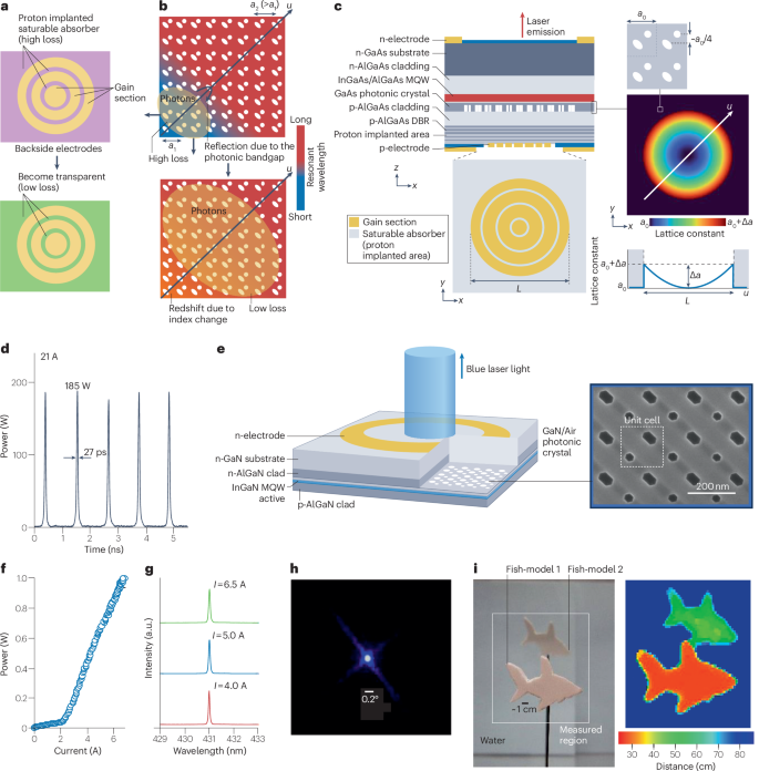
a, Schematic of a short-pulse photonic-crystal surface-emitting laser (PCSEL) with 2D arranged gain and loss sections23. b, Schematic of a short-pulse PCSEL with a self-evolving photonic crystal24. c, Schematic of a 200-W-class short-pulse PCSEL combining 2D arranged gain and loss sections and a self-evolving photonic crystal. d, An example of the pulsed operation of the short-pulse PCSEL shown in panel c43. e, Schematic diagram of a GaN-based short-wavelength PCSEL. The inset shows a scanning electron microscope image of the fabricated photonic crystal. f–h, I–L characteristics (panel f), lasing spectra (panel g) and far-field pattern (panel h) at 6.5 A, demonstrating watt-class, high-beam-quality operation of a short-wavelength PCSEL25. i, Demonstration of underwater time-of-flight light detection and ranging (ToF-LiDAR) using a short-wavelength PCSEL. The left panel shows a photograph of the evaluation targets in water, and the right panel shows a corresponding underwater distance image. DBR, distributed Bragg reflector; MQW, multiple quantum wells. Panels c and d adapted with permission from ref. 43, Optica Publishing Group. Panels e–g adapted from ref. 25, CC BY 4.0 (https://creativecommons.org/licenses/by/4.0/).
Aside from the PCSELs with gain and loss sections, another concept, the ‘self-evolving photonic crystal’, was also proposed to realize Q-switching operation in PCSELs24. Qualitatively, the band-edge resonant frequency distribution within this photonic crystal dynamically changes during lasing oscillation, inducing a spontaneous decrease of the cavity loss akin to the case of Q-switched lasers with gain and loss sections. In the self-evolving photonic-crystal, the lattice constant is continuously increased along the diagonal axis inside the gain region (Fig. 4b). In this photonic crystal, the gradation of the lattice constant induces the band-edge resonant frequency distribution, and the photons cannot spread over a wide area, owing to the photonic mode gap. Instead, the photons are confined in the corner of the gain region (Fig. 4b, upper panel) and the in-plane loss of the resonant mode significantly increases. However, when the lasing oscillation starts, the gradation of the band-edge frequency is dynamically compensated because the carrier density decreases during stimulated emission and the refractive index increases (Fig. 4b). Consequently, the confinement due to the mode gap is weakened, and the light propagates into the neighbouring broader section with many accumulated carriers, by which the light is further amplified24.
The latest PCSELs combine the concept of 2D gain and loss sections with that of the self-evolving photonic crystal (Fig. 4c). A 200-W-class peak power and a pulse width of less than 30 ps were successfully demonstrated43 (Fig. 4d). Note that when this PCSEL is excited by a nanosecond electronic pulse, only one short, high-peak-power pulse can be generated, and this excitation can be repeated at a desired time interval, for example once per microsecond. In the future, even higher peak powers (>1 kW) will be realized by enlarging the photonic crystal and by optimizing the design of the gain and loss sections and/or the band-edge frequency gradation. These short-pulse, high-peak-power PCSELs are expected to find applications in the next-generation long-distance, all-electronic, non-mechanical LiDAR as well as in non-thermal laser processing and bioimaging using multiphoton processes.
Next, we explain GaN-based PCSELs operating at short wavelengths (~430 nm) (Fig. 4e), as an example of the extension of emission wavelength rage of PCSELs14,25,31,50,51,52,53,54,55. A GaN-based PCSEL was first demonstrated in 200814. In 2022, watt-class operation of a GaN-based PCSEL was successfully achieved25. In this PCSEL, a 300-μm-diameter double-lattice photonic-crystal structure was used by adjusting the lattice spacing of the individual lattices to enhance optical confinement within the plane of the photonic crystal25. This enhanced confinement compensated the low refractive-index contrast in GaN-based PCSELs, compared with that in the GaAs-based PCSELs18,19,20. A double-lattice structure was also used to introduce asymmetry to the unit-cell structure to enhance the vertical emission18,25. Scanning electron microscope characterization of the fabricated GaN-based photonic crystal (inset of Fig. 4e) revealed the formation of a uniform photonic-crystal structure, where the two air holes of the double-lattice were elongated and symmetric hexagons.
Figure 4f shows the output power as a function of injection current for the 300-μm-diameter PCSEL under pulsed operation. A threshold current of 2.1 A (threshold current density of 3.0 kA cm−2) was measured, which was 22 times smaller than that of the first demonstration of GaN-based PCSELs. A single-mode output power of over 1 W at a wavelength of 431 nm was successfully obtained (Fig. 4g). The far-field pattern observed at an injection current of 6.5 A (Fig. 4h) indicates a narrow divergence angle of 0.15°. These results clearly demonstrate the achievement of high-brightness operation using GaN PCSELs, which is not feasible using existing GaN lasers.
One unique example of the applications of high-brightness GaN PCSELs is an underwater LiDAR system. Water absorbs near-infrared wavelengths of light much more strongly than blue wavelengths. For this reason, a PCSEL-LiDAR system operating at 940 nm cannot be used underwater. Underwater ranging of two fish models at different distances has been successfully achieved with GaN-PCSEL-based LiDAR (Fig. 4i). Remarkably, even underwater LiDAR does not require a complicated lens system, thanks to the high brightness of the GaN PCSELs.
GaN PCSELs can be also operated under CW conditions with single-mode output powers of over 320 mW (ref. 25). In the future, even higher output powers (above 10 W or even 100 W) with high beam qualities could be achieved by further increasing the resonator diameter (to 1 mm and beyond) by adjusting the lattice spacing of the double-lattice structure to achieve destructive interference that weakens in-plane confinement (Fig. 2e). Following this strategy, GaN PCSELs can be applied to the processing of difficult-to-process materials, including carbon-fibre-reinforced plastic (CFRP) and copper. Laser processing of CFRP and copper is expected to become increasingly valuable for realizing carbon-neutral transportation. GaN PCSELs could also find use in adaptive driving beams and laser displays.
Summary and outlook
Recently, there has been remarkable progress in high-brightness and high-functionality PCSELs, setting new research trends. Using double-lattice photonic crystals, at first under pulsed conditions, the brightness of PCSELs has reached 1 GW cm−2 sr−1. Class-minimum LiDAR for smart mobility of robots has been demonstrated using high-brightness 500-μm-diameter PCSELs. Furthermore, it has been successfully demonstrated that PCSELs can be fabricated based on nanoimprinting technology, showing potential for mass production. The reliability of PCSELs has also been confirmed.
The brightness reached 1 GW cm−2 sr−1 even under CW conditions in 3-mm-diameter PCSELs with controlled Hermitian and non-Hermitian coupling coefficients, leading to the cutting of stainless steel. The obtained CW brightness is comparable to that of bulky lasers such as gas and solid-state lasers. A 3-mm-diameter PCSEL can operate even at a 1-kW power level under pulsed conditions as well, leading to the realization of colour marking of stainless steels with various colours ranging from grey to yellow. In the near future, CW kilowatt-class operation is expected to become possible by expanding the laser diameter from 3 mm to 10 mm and optimizing Hermitian and non-Hermitian coupling coefficients, which will enable a further 10-to-100-fold improvement in the output power and beam brightness.
High-functionality operations of PCSELs based on modulated photonic crystals have been demonstrated, such as wide-range 2D beam-scanning operation using an integrated chip with modulated PCSELs, and even the generation of various beam shapes without the use of any external optics. We propose that this technology will lead to various applications including all-electronic non-mechanical LiDAR, face and object recognition, compact displays of arbitrary pictures, and even high-throughput material processing.
Finally, we have identified two new trends of PCSELs. One direction is short-pulse (<100 ps), high-peak-power (>100 W) PCSELs, based on a combination of 2D saturable absorbers and self-evolving photonic crystals. Such PCSELs are expected to be applied to next-generation long-distance all-electronic, non-mechanical LiDAR, as well as non-thermal laser processing and bioimaging using multiphoton processes. The other trend is GaN PCSELs, capable of short-wavelength (blue, approximately 430 nm), watt-class operation under pulsed conditions; for underwater LiDAR applications. Considering the ability of GaN PCSELs to operate under CW conditions, we believe that in the future, these PCSELs will be applicable to the processing of difficult-to-handle materials, including CFRP and copper, as well as illumination including adaptive driving beams and laser displays.
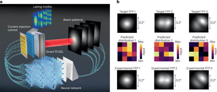
Ongoing advanced research on PCSELs includes their integration with artificial intelligence (AI) technology based on machine learning and their design based on quantum technologies. Smart PCSELs integrated with AI are capable of on-chip lasing-mode control (Box 2). Here, the relationship between the current injection distribution and the beam pattern is learned by a neural network (panel a of the Box 2 figure), enabling emission of a beam with desired (or targeted) modes (panel b of the Box 2 figure). Design optimization of PCSELs using quantum annealing has been also used27 to optimize the shape of the photonic-crystal air holes, the injection current distribution and the resonant frequency distribution inside the PCSELs to increase the output power, to shrink the divergence angle and to increase the linear polarization ratio with respect to conventional, uniform PCSELs.
In summary, PCSELs boast both high brightness and high functionality while maintaining the merits of semiconductor lasers, and thus they offer solutions to the issues of existing laser technologies. PCSELs even incorporate new technologies, such as AI and quantum technologies. The potential applications of PCSELs are diverse, including not only smart mobility and smart manufacturing as described above, but also communications, mobile technologies, medicine, biology and even aerospace. In aerospace, the compact, high-brightness nature of PCSELs is advantageous for intersatellite communications56,57. When their brightness is further increased to realize ultrahigh-power emission, PCSELs can even be used for laser propulsion of spacecraft58 and as light sources for extreme-ultraviolet lithography and laser fusion. The remaining challenges in PCSEL development include the realization of a large-area (10-mm-diameter or even larger), single-mode PCSEL to enable such exotic applications. In these and many other ways, PCSELs are anticipated to contribute to future society.
Responses