Photorefractive and pyroelectric photonic memory and long-term stability in thin-film lithium niobate microresonators

Introduction
Lithium niobate (LN), first discovered in 1949 as a ferroelectric crystal, has been known for its excellent optical properties including such as large electric-optic (EO) coefficient, second and third-order optical nonlinearities, and a wide transparency window from 0.3 to 5.5 μm1,2,3. The recent advancement of the low-loss thin-film-lithium-niobate (TFLN) photonic devices has enabled compact high-performance frequency converters4,5, EO6,7 and acousto-optic modulators8 on a monolithic platform, which quickly attract significant interest for building the future integrated photonic circuits. However, the scalability and reliability of the TFLN platform remains an open but critically important question with many technical challenges to be solved, such as intra-device drift, inter-device variation and fabrication inhomogeneities.
Figure 1a shows that the temporal variation of the optical refractive index would lead to the drift of the bias voltage in the EO modulators which degrades the health of the classical and quantum optical communication links9,10 as well as the drift of the cavity resonance position which disrupts the measurement required at a certain pump-cavity detuning11. Despite the studies of the bulk LN material12, the TFLN platform shows different behaviors from its bulk form due to the tighter optical confinement, the condition of surface defects and nanofabrication process13,14. Compared to the more matured photonic material, such as silicon or silicon nitride, the LN exhibits far richer material properties, such as birefringent, photorefractive (PR), photovoltaic and pyroelectric (PE) effect. Photorefractive effect is a result of the photovoltaic effect through optically pumping the trapped electrons from the impurity level to the conduction band (Fig. 1b) while pyroelectric effect describes the change of the spontaneous polarization of the material as a result of temperature change ΔT (Fig. 1c), both of which give rise to a built-in electrical field along the crystal axis as sketched in Fig. 1d. The change of the optical refractive index is proportional to the product of the EO coefficient and the resulting electric field. Therefore, experimental characterization of the PR and PE effects is essential to understand the systems which need to operate at high optical power15 or be cooled to cryogenic temperature10, rely on thermo-optic effect for tunability16,17,18 and are sensitive to the carrier dynamics such as superconducting detectors19,20. There are recent reports on the fast time oscillation of the PR effect13,21,22 and the thermo-refractive noise23. However, the long-term stability of the optical properties has not been studied on the TFLN platform. In addition, non-volatile photonic memory24 has not been reported in TFLN devices despite the photorefractive effect is routinely used for holographic data storage in bulk LN crystals25,26.

a The change of the optical refractive index ((varDelta n)) could lead to the transmission variation due to the resonance frequency drift of an optical cavity or the bias-voltage drift of an amplitude electro-optic (EO) modulator. b Electrons from the impurity level is optically excited into the conduction band by the photorefractive (PR) effect; c Temperature change induces electrical current by the pyroelectric (PE) effect, ({P}_{s}): spontaneous polarization of the material; d Carriers from either the PR or PR effect lead to a built-in electrical field (({E}_{{rm{built}}-{rm{in}}})) in the TFLN waveguide which results in (varDelta n) via the EO effect of LN ((varDelta npropto {E}_{{rm{built}}-{rm{in}}}cdot {gamma }_{{rm{EO}}}), ({gamma }_{{rm{EO}}}): the EO coefficient).
In this paper, we systematically investigate the PR and PE effects and their temporal dynamics in both X-cut and Z-cut TFLN devices. The change of the optical refractive index is monitored using the transmission spectrum of high quality-factor microresonators. Due to the electron trapping at the surface defect states and the thin feature of the film, the built-in electric field is found to be stronger and takes significantly longer time to decay when the crystal axis is perpendicular to the device plane (Z-cut), in comparison with the X-cut device with a similar dimension. In Z-cut TFLN microresonators, we observe a blue-shifted cavity resonance with a recovery time of over 20 h after optical excitation is turned off. Leveraging the long lifetime, we achieve deterministic and controllable frequency shifting of the resonance frequency via controlling the injected light, and trimming different devices to resonant at identical optical frequencies. Moreover, we find that the joint PE and EO effect causes the optical resonance to blue shift upon increasing the device temperature. The time scale of the process is dominated by the charge dynamics and differs significantly from the thermal dynamics. Similarly, a long recovery time of over 10 h is observed. Our work is of importance to understand the stability of the TFLN photonic devices for both classical and quantum applications. The long-lived PR and PE effect could also be used for realizing non-volatile optical memory and overcoming fabrication inhomogeneity as well as for optical sensors27 and bolometers28.
Results
Approach
The devices are air cladded and fabricated on a 600-nm LN wafer with an etch depth of 350 nm, a top width of 1.5 µm and a bending radius of 80 µm. The cross-section and scanning electron microscope images are shown in Fig. 2a. Figure 2b shows the transmission spectrum of the microresonator via sweeping the frequency of a continuous-wave laser. The intrinsic Q factor is extracted to be (3.3times {10}^{6}) at near 1560 nm for the fundamental transverse-electric (TE) mode. Both X-cut and Z-cut LN microrings with the same geometry are fabricated for comparative analysis. The effective refractive index change ((varDelta {n}_{{rm{eff}}})) can be extracted by measuring the optical resonance shift of microrings based on
where ({n}_{{rm{eff}}}) is the effective refractive index for light propagating in the ring waveguide.
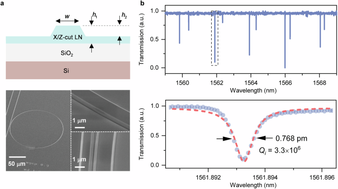
a Cross-section schematic and the scanning electron microscope (SEM) of the microresonators. The waveguide height ({h}_{1}), 600 nm; the etch depth ({h}_{2}), 350 nm; the waveguide top width (w), 1.5 µm. b Transmission spectrum. The extracted intrinsic Q factor (Qi) to be 3.3 million.
Photorefractive effect characterization
To study the photorefractive induced refractive index change, we control the sweeping parameter of a continuous-wave control laser across the resonance to introduce photorefraction, and measure the optical resonance shift using a second probe laser at low optical power in the meantime (see Methods). The wavelengths of both lasers are scanned from the short to the long wavelength, as shown in Fig. 3a. The device is placed on a thermo-electric-controller (TEC) to keep a constant temperature. The optical power of the control laser in the waveguide is 80 mW. The detailed setup is shown in Fig. S1 in the supplementary file. After 500 cycles of the control laser sweeping at a 5-nm/s speed across a 20-pm spectral range, a total cumulated wavelength shifts of −13.7 pm is achieved via the PR effect (Fig. 3b) corresponding to a (varDelta {n}_{{rm{eff}}}) of (-1.8times {10}^{-5}). The index is preserved after the control light is turned off, indicating a photonic memory effect which has not been reported before.
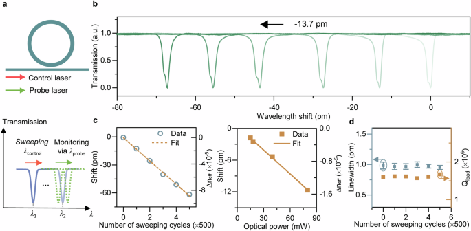
a Schematic of the PR characterization. A control laser is used to sweep the resonance, after which the probe laser is to monitor the resonance shift. b Resonance blueshifts during 2500 sweeping loops, each 500 cycles induce −13.7 pm wavelength shift. c Resonance wavelength shift ((varDelta n)) as a linear function of the number of sweeping cycles (at 80-mW on-chip optical power) and the on-chip power (with 430 cycles). d Loaded linewidth and the loaded Q factor during the 2500 sweeping cycles.
Figure 3c plots the resonance shift (and(varDelta n)) is linearly proportional to the number of the sweeping cycle and the control laser power, thus the total injected optical energy. The largest refractive index change we demonstrate in this work is (-8.6times {10}^{-5}). One can estimate the internal electrical field strength ({E}_{{rm{built}}-{rm{in}}}) along the polarization axis to be (1.7times {10}^{6}) V/m based on the effective refractive index change:
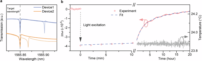
where ({n}_{0}) and ({r}_{13}) are the LN ordinary optical refractive index and the EO coefficient (9.6 pm/V)29, respectively. We also verify that the optical loss of the device didn’t deteriorate by monitoring the Q-factor during the process (Fig. 3d). Furthermore, we demonstrate the PR-based tuning for two different rings, both of which are trimmed to have the same resonance wavelength of 1565.85 nm by a blue shift of 53 pm ((varDelta {n}_{{rm{eff}}}=-6.7times {10}^{-5})) and 17 pm ((varDelta {n}_{{rm{eff}}}=-2.2times {10}^{-5})), respectively (Fig. 4a). The non-volatile tuning shows promises for post-fabrication trimming of photonic circuits. Next, we study the temporal stability of the PR-induced effect. Figure 4b plots the refractive index change over time including the PR excitation induced by the control light and subsequent relaxation after the control light is turned off, and we did not observe the continued blue shifted resonance. As shown in Fig. 4b, the cavity resonance drifts over one cavity linewidth (~1 pm in our case) over a 10-min time period. This can serve as a figure of merit for defining the effective operational time for the memory application. As we continue to track the shift over a time window of 20 h, we observe that the resonance position slowly moves towards the original wavelength due to the space-charge field relaxation. After 20 h, the optical index doesn’t restore to the initial value. This process can be described by
where (t) is the time, ({partial }_{1}) and ({partial }_{2}) denote the wavelength shift before recovery, ({tau }_{1}) and ({tau }_{2}) are characteristic time constants. The time constants ({tau }_{1}) and ({tau }_{2}) are fitted to be 1.69 and 10.06 hours respectively, five orders of magnitude longer than the reported values in the X-cut LN13,21,22. The detailed analysis and comparison are shown in the discussion section. The large time constant could be leveraged to realize temporary optical memory on chip.
a Optical resonance trimming via the PR effect. b Temporal dynamics of the optical refractive index. PR effect shows a relaxation process over a duration of 20 h with a change of one cavity linewidth (~1 pm) within the first 10 min window.
Pyroelectric effect characterization
We characterize the pyroelectric effect by changing the device temperature using the TEC while tracking the resonance position using the same probe laser (see Methods). The temperature variation (Delta T) modifies the position of the atoms within the crystal and thus changes the polarization of the LN material, generating a voltage across the thin film LN via the PE effect. The resulting electrical field is given by
where ({p}_{{rm{s}}}) is the spontaneous polarization, (p=frac{partial {P}_{{rm{s}}}}{partial T}) represents the pyroelectric coefficient of LN ((Ccdot c{m}^{2}cdot ^{circ} {C}^{-1})), ({varepsilon }_{0}) and ({varepsilon }_{{rm{r}}}) denote the free space permittivity and relative dielectric permittivity, respectively. Therefore, the (varDelta {n}_{{rm{eff}}}) via the PE and EO effect can be estimated using Eq. (2), indicating a negative relationship between (varDelta n) and (varDelta T). We note that the thermo-optic (TO) effect would take place concurrently and contribute to a positive change of the index with an increased temperature. ((varDelta n=dn/dTcdot varDelta T), where (dn/dT) is the TO coefficient30,31).
Figure 5a plots the resonance shift and the index change as a function of time at a temporal resolution of 3 s over a 30-min window, while we apply a temporal pulse of temperature with a peak temperature of 54 °C. We observe a dynamic resonance shift with four stages as labeled in Fig. 5a: (1) the resonance blue shifts proportional to the temperature difference ((Delta T, >, 0)) due to the PE and EO effect; (2) the resonance starts to red shift due to the slower TO effect; (3) the resonance experiences a sharp transition of red shift due to the negative (varDelta T) (<0) and the PE; (4) resonance blue shifts due to the TO effect as the temperature goes back to the room temperature, and continue to blue shift due to the slow relaxation of PE-induced carriers. It is clear that the TO and PE are distinct from each other in terms of shifts and the time scale, as the TO effect is determined by thermal dissipation while the PE effect is related to the carrier relaxation dynamics (likely due to the surface charge neutralization through the air). For clarity, we show the corresponding transmission spectra for these stages in Fig. 5b.
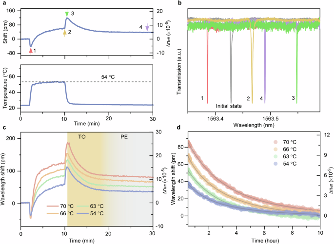
a Resonance shifts over 30 min under excitation of a temperature pulse. b The transmission spectra of four stages labeled in (a). c Temporal dynamics with four different temperature pulses. The two shaded regimes represent processes dominated by the TO and PE effects, respectively. d PE relaxation process over 10 h.
Figure 5c shows the temporal dynamics under pulses with different peak temperature values of 54, 63, 66, and 70 °C, respectively. We extract the PE-induced (dn/dT) to be (-2.9times {10}^{-6}/^{circ} C). In the final (4th) stage, there are two different decay times, one of which is relatively fast attributed to the TO effect (shaded in yellow). The slow decay (shaded in gray) is due to the PE effect. Figure 5d shows the recovery time for the PE effect to be over 10 h. The fitted time constants are shown in Table S1. This result presents the first characterization of the PE effect and its long-term stability in the TFLN platform. It is of importance for applications including chip-based temperature sensor and bolometer.
Discussion
Finally, we perform similar investigation in the X-cut microresonators of the same dimension. In the PR experiment, the long-term relaxation and the memory phenomenon is no longer observable in the X-cut device and the optical resonance goes back to the initial position after the control laser sweep. Instead, we observe the distortion of the optical resonance transmission as we bidirectionally scan across the resonance (Fig. S2) regardless of X- or Z-cut. This is a result of the PR effect at a faster time scale, which competes with the TO effect13,21,22. It is observed that the PR effect is more pronounced in the Z-cut device, while the TO effect is more dominant in the X-cut device, resulting in the distinct resonance transmission by sweeping the laser wavelength at higher power. Similarly, the long-term instability of the PE effect is also absent in X-cut devices and the refractive index change follows the thermal dynamics (Fig. S3). Therefore, the memory effect strongly depends on the crystal orientation and poses challenges deploying the Z-cut TFLN devices for precision optical measurement, suggesting that active feedback circuits might be necessary. Utilizing balanced arms in the Mach-Zehnder-interferometer-based modulators would help cancel out the index change difference between two arms. Moreover, it is worthy to note that the resulting internal electric field is stronger as one further shrinks the physical dimension of the device, which explains distinct behaviors from its bulk form. The slow recombination of the electrons at the surface could explain the long relaxation time of optical refractive index observed on the Z-cut devices. We envision that applying conductive coating to neutralize the surface charge12,14 or ion doping25 could further reduce the recovery time or erase the optical memory. Furthermore, the induced electrical field should be of relevance to the optical poling of the LN32 as well as the acoustic circuit operation via piezoelectricity33.
In summary, we demonstrate a temporary photonic memory effect induced by light and temperature excitation through the photorefractive, pyroelectric and electro-optic effects based on the high-Q TFLN microresonators. Long-lived optical refractive index change over hours is observed and characterized in the Z-cut TFLN, showing distinct behaviors from the X-cut TFLN and revealing the temporal dynamics of the charge dissipation. Taking advantage of the long-lived feature, non-volatile trimming of TFLN microresonators is demonstrated, for the first time, via a precise control of light excitation. Our work is an important step towards building a practical, scalable and reliable TFLN photonic platform in the future.
Methods
Photorefractive effect characterization and measurement
To characterize the photorefractive induced refractive index change, we utilize a high-power control for light excitation and a low-power probe laser for monitoring. The control laser output power is amplified and adjusted using an erbium-doped fiber amplifier. Two wavelength division multiplexers are used to combine and separate the control and probe light, operating near 1546 nm and 1550 nm, respectively. A polarization controller and a polarizer are utilized to ensure TE-mode excitation in the waveguide. The transmitted control light is monitored with a power meter, while the transmission spectrum of the probe light is recorded via a data acquisition card. The device under test is placed on a thermoelectric cooler (TEC) to keep at a stable temperature, preventing temperature-induced drifts during the photorefraction measurement. The wavelength of the control laser is scanned across the resonance from the short to long wavelength to introduce photorefraction, while the probe laser wavelength is continuously swept in the meantime to obtain the transmission spectrum.
Pyroelectric effect characterization and measurement
The characterization and measurement of the pyroelectric effect are performed using a similar setup to the photorefractive measurement, with the addition of a TEC for controlled temperature variations. Different temperature pulses are applied by controlling the voltage supplied to the TEC. A low-power CW probe laser is scanned continuously to track the resonance shift induced by temperature changes.
Responses