Physics-informed Bayesian optimization suitable for extrapolation of materials growth

Introduction
Integrating machine learning techniques, including Bayesian optimization (BO) and artificial neural networks, into materials science has ushered in a new era of research1,2,3. This paradigm shift revolves around data-driven decision-making approaches that enable high-throughput experiments, wherein machine learning models are incrementally updated with newly acquired data4,5,6. Here, Bayesian optimization (BO), a sample-efficient approach for global optimization7, is a powerful tool for optimizing the synthesis conditions of both bulk8 and thin film materials9,10,11. BO algorithms suggest growth conditions for the next experimental run based on predictions from past observations. The entire process, combining BO with automated growth and characterization instruments12,13, has been automated in a number of ways, and these approaches are collectively referred to as autonomous materials synthesis14,15.
Recently, efforts to construct machine learning models utilizing physics-based prior knowledge have been referred to as physics-informed machine learning and various endeavors have been made in this regard16,17. The ability to use prior knowledge in BO is also essential; in fact, it is crucial to the success or failure of an optimization. However, Gaussian process regression (GPR), the prediction model used in BO, is unsuitable for extrapolation prediction. This situation has led to the existing data sets being not very useful for optimizing experiments in conditions not included in the existing datasets. This difficulty is a common issue encountered in machine learning-based predictions in general. To address this problem, incorporating prior knowledge, such as extrapolable physics models, into GPR models is expected to expedite the experimental optimization process.
In this study, we propose a physics-informed Bayesian optimization (PIBO) method that utilizes prior physics knowledge, particularly Vegard’s law and the linearity between gas flow rate and composition in compound semiconductors. By applying this method to metal-organic chemical vapor deposition (MOCVD), we succeeded, throughout a small number of experiments, in synthesizing III–V semiconductors with the desired band gap wavelengths and lattice constants in a region not included in existing growth datasets. These results demonstrate that even if the predictive model itself cannot be extrapolated, an extrapolable machine learning model having a wide range of applicability can be constructed by incorporating robust physics knowledge. Moreover, PIBO predicted hidden trends in the crystal growth phase diagram that were not in prior physics knowledge, showing that statistical machine learning aids not only optimization but also understanding of crystal growth mechanisms. Combining such physics knowledge with machine learning models to build extrapolable physics-informed machine learning models will be critical for improving the efficiency of high-throughput materials growth and autonomous materials synthesis.
Results
Physics-informed Bayesian optimization (PIBO)
As a stage for developing the PIBO model using prior physics knowledge, we chose the compound semiconductor system In(1-x)Ga(x)As(y)P(1-y) (0(le)x(le)1, 0(le)y(le)1) (InGaAsP) on InP substrate. InGaAsP is widely employed in various optical components, such as semiconductor lasers, optical modulators, and optical amplifiers relating to fiber optics systems, and thus, synthesizing InGaAsP having the desired optical properties is an issue of industrial importance. InGaAsP layers with specific compositions, x and y, are grown by adjusting the flow rates of the In, Ga, P, and As gases18. The compositions specify the band gap wavelength (({lambda }_{g})) and lattice constant (d) of the synthesized InGaAsP layers. To utilize InGaAsP in optical components for light emission and absorption at ({lambda }_{g}), we need to grow the epitaxial InGaAsP layers whose ({lambda }_{g}) and d are optimized to the purpose at hand.
Our goal is to make ({lambda }_{g}) and d close to the target design values simultaneously. To this end, we adjusted the flow rates of Ga and As gases, while maintaining those of In and P to control the composition, i.e., x and y, of the resulting compound. The search process for appropriate flow rates is challenging in two ways. First, the gap in the numerical scale of the physical properties (({lambda }_{g}) and d) affects their simultaneous optimization. Typically, an optimization algorithm will focus on the metric with the greater scale, whereas it tends to ignore the metric with the smaller scale. Second, since a complex crystallization process is involved, the physical properties may be difficult to derive from the flow rate values, hindering the optimization of ({lambda }_{g}) and d. We deal with these difficulties by incorporating prior physics knowledge into the BO framework. Specifically, we convert ({lambda }_{g}) and d (the target values) into equivalent x and y compositions (the target compositions) via Vegard’s law to meet the first challenge (Fig. 1a). This conversion is advantageous in that x and y share the same scale, having a range between 0 and 1. Second, we encourage monotonic relationships between FGa [sccm] (the flow rate of Ga) and x, and similarly between FAs [sccm] (As flow rate) and y. This choice is motivated by the fact that MOCVD growth is controlled and limited by molecular transport and adsorption at the growth surface18 (Fig. 1b).

a Example of conversion from ({lambda }_{g}) and d to x and y via Vegard’s law for six data points (N1-N6 InGaAsP layers). b Schematic diagram of the growth surface. MOCVD growth progresses as material gas molecules (blue circles), which follow a Maxwell velocity distribution, adsorb onto the growth surface.
Vegard’s law provides the relationship between the composition ratios, x and y, and the measured characteristics, ({lambda }_{g}) and d. Principally, Vegard’s law including the bowing parameter can be expressed as follows19,20,21.
Here, Eg is the band gap energy of the grown InGaAsP layer. We can convert a pair of physical values (scriptstyleleft({lambda }_{g},dright)) into (left(x,yright)) values by using a numerical root-finding method such as Newton’s method22. Subsequently, x and y can be obtained by measuring λg and d. For this reason, we can define the datasets consisting of the flows of the material gases and the compositions of the grown layer (FGa, FAs, x, y).
We use the following prediction model to enhance the monotonic relationship between FGa and x:
where we impose ({a}_{0}ge 0) to encourage the increase in x as FGa increases. A similar prediction is made for y:
where ({a}_{1}ge 0). A Gaussian process (GP) is used to model the residual components ({r}_{0}) and ({r}_{1}). Since the interaction of gas flows FGa and FAs may be complex, GP better fits the residual terms beyond the linearity relationship between composition ratios and gas flows. Strictly speaking, x may not be monotonically increasing with ({F}_{{rm{Ga}}}) even when ({a}_{0}ge 0) because the ({r}_{0}left({F}_{{rm{Ga}}},{F}_{{rm{As}}}right)) term may decrease with ({F}_{{rm{Ga}}}). In practice, we found that we can suppress the amplitude of ({r}_{0}) and ({r}_{1}) by performing the following estimation steps.
Let ({{mathcal{D}}}_{N}:= {left{left({F}_{{rm{Ga}}}^{n},{F}_{{rm{As}}}^{n},{x}^{n},{y}^{n}right)right}}_{n=1}^{N}) be the observed variables in N experiments with n being the observation index. Note that, in our case, the raw observations, ({lambda }_{{rm{g}}}^{n}) and ({d}^{n}), are converted into ({x}^{n}) and ({y}^{n}) by Vegard’s law (Eqs. (1)—(3)). We build the following prediction model for x and y at arbitrary FGa and FAs, based on GP and utilizing ({{mathcal{D}}}_{N}):
Note that x and y may not be independent. Nevertheless, we chose this model since a limited amount of observed data prevents a reliable fitting of more general models that take into account the dependence of x and y.
This prediction model is used to calculate acquisition values that determine a pair of parameters (left({F}_{{rm{Ga}}}^{N+1},{F}_{{rm{As}}}^{N+1}right)) for the next experiment. Simply put, a low acquisition value indicates that the rescaled distance between the predicted values of (x, y) and their respective targets is likely to be close to zero. Therefore, we choose the next experimental conditions for FGa and FAs with the lowest acquisition value (see the Methods section “Bayesian optimization for target values” for more details). The prediction model incorporates physics knowledge in two ways to overcome the difficulties of the naive application of BO for matching target values. First, Vegard’s law alleviates the scale mismatch between multiple target values by converting the physical quantities into normalized target compositions. Second, the linear relationship between the flow rate and resulting composition effectively extrapolates the prediction to the entire search space, even its unexplored regions. The PIBO algorithm enjoys efficient optimization performance by making reliable predictions of regions not included in the existing dataset, unlike ordinary BO, which may suffer from biased predictions in unexplored regions.
Application of PIBO method to MOCVD of InGaAsP system
We applied the PIBO method to the MOCVD growth of InGaAsP on an InP substrate to demonstrate its applicability and effectiveness. Fig. 2 shows the flow of PIBO in the case of MOCVD growth (see Methods section “MOCVD, PL, and X-ray diffraction setups” for details of experimental setups). First, the InP substrate is put on a susceptor, and material gases flow into the reactor (Fig. 2a). The growth temperature is set to 650 °C, as is generally done for InGaAsP. The In, Ga, As, and P gas compositions are controlled by mixing them with H2 carrier gas; the material gases are transported through a gas line (see Sec. I of the Supplementary information for more details). The In, Ga, As, and P gas flow rates are denoted as FIn, FGa, FAs, and FP (Fig. 1a). In the experiment, FIn and FP were fixed, and only FGa and FAs were varied to obtain the target compositions. After the MOCVD growth at a certain FGa and FAs, λg and d of the grown layer were evaluated by measuring the photoluminescence (PL) wavelength and performing X-ray diffraction (XRD) (Fig. 2b), and the dataset (Fig. 2c) was updated. Then, the GP model utilizing Vegard’s law and the linear relationship between gas flow rate and composition was updated using the dataset. Subsequently, the acquisition value was calculated to assign the FGa and FAs values in the next run (Fig. 2d). Hereafter, we refer to the growth run numbers as N1, N2, etc.
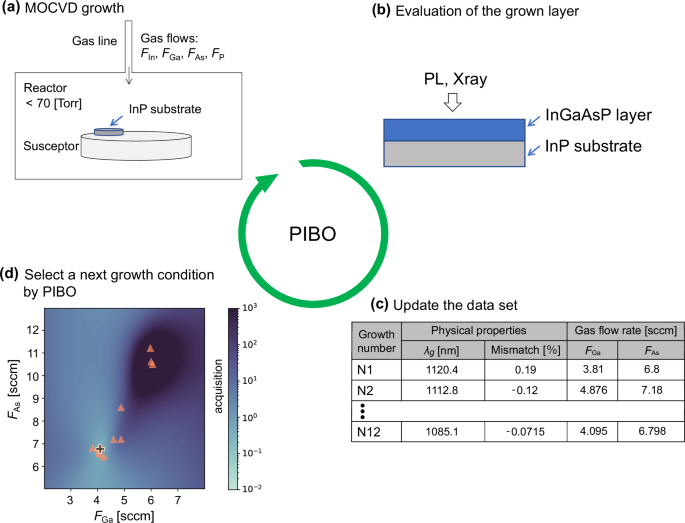
a, b Schematic illustration of (a) MOCVD setup and (b) evaluation of the grown layer. c Physical properties (({lambda }_{g}) and the lattice mismatch between the grown InGaAsP layer and the InP substrate (frac{(dmbox{-}5.8688)times 100}{5.8688}) [%]) and growth conditions (FGa and FAs) for 12 samples (N1-N12 InGaAsP layers), as an example. d Two-dimensional plots of acquisition values obtained from the collected data for 12 samples (N1-N12 InGaAsP layers), as an example.
Here, we describe how the composition of individual samples is determined from PL and XRD data. Figure 3a, b shows the PL spectrum around the center of the N1 InGaAsP layer and the PL wavelength map of that layer on the InP wafer, as an example. We took the average value of the PL wavelength map to be the PL wavelength. In this example, the average PL wavelength of the N1 InGaAsP layer is 1120.4 nm. Figure 3c shows the XRD (theta)-2(theta) pattern of the same InGaAsP layer. Here, the XRD peak position can be used to estimate the value of d of the N1 InGaAsP layer. The XRD fringes originated from multiple reflections at the interfaces between the buffer InP and InGaAsP, and the InGaAsP layer and cap InP. Here, to calculate the lattice constant from the XRD measurement, we need to consider strain relaxation because the thickness of the epilayer affects the residual strain, which in turn affects the calculated lattice constant23. In this study, we estimated the lattice constant under the assumption that the epitaxial layer had relaxed. The target composition of the InGaAsP layer was chosen so that the lattice constant of the target InGaAsP layer matched that of the InP substrate. Therefore, when the composition of the grown InGaAsP is close to the target composition, strain relaxation does not occur, and the above assumption does not affect the estimation of the lattice constant (see Sec. II of the Supplementary information for more details). In this example, Vegard’s law determined x and y of the N1 InGaAsP layer to be 0.1124 and 0.3043, respectively.
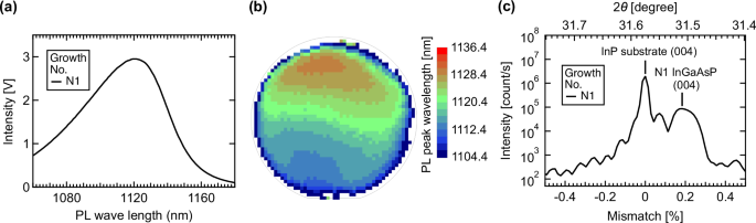
a Photoluminescence (PL) spectrum measured at the center of the N1 InGaAsP layer. b PL spectrum mapping of the N1 InGaAsP layer. The calar scale represents the peak position of the PL spectrum at each position. We took the average value of the PL wavelength map to be the λg of the sample. c θ–2θ scanned XRD pattern of the N1 InGaAsP layer.
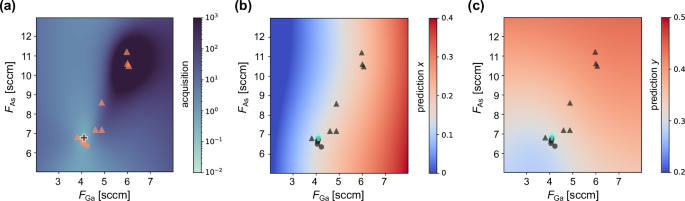
To examine the effectiveness of the PIBO method in extrapolating MOCVD growth conditions, we prepared a preliminary dataset consisting of six samples (N1-N6 InGaAsP layers) with λg in the range of 1120.4 nm – 1162.7 nm and used PIBO to fabricate InGaAsP with λg = 1180 nm, a wavelength not included in the range of the preliminary data. Here, the termination requirements for optimization were that λg be (pm)10 nm of the target value and the lattice mismatch between the grown InGaAsP layer and the InP substrate (frac{(dmbox{-}5.8688)times 100}{5.8688}) [%] be (pm)0.05%. The latter requirement arises from the need for the InGaAsP layer to be lattice-matched to the InP substrate. This ensures optimal performance and compatibility between the layers in actual optical devices. This target (scriptstyleleft({lambda }_{g},dright)) = (1180, 5.8688) corresponds to (left(x,yright)) = (0.1953, 0.4247) (First target compositions). Figure 4 shows the resulting predictions in the {FGa, FAs} growth parameter space with the six preliminary datasets. As a result of incorporating the physics knowledge on the relationships between gas flow rate and composition, as expressed by Eqs. (4)-(5), into the prediction model, the predicted values of x and y monotonically increased with the values of FGa and FAs (Fig. 4b, c). The monotonically increasing relationship existed even in regions without any experimental data, meaning that the predictions were suitable for extrapolation. This monotonically increasing behavior is not predicted by the naive GPR prediction, which does not take into account the monotonic relationship as prior knowledge (see Sec. III of the Supplementary information for more details). The white areas in Fig. 4b, c represent the regions containing the target x and y values. Hence, as shown in Fig. 4a, a low acquisition value was obtained in the region of overlap between the two white areas, wherein the target x and y values were predicted to be simultaneously obtained. The values in these regions were thus selected as the growth conditions for the next experiment [{FGa, FAs} = {5.972, 11.2}]. Based on the linear relationship between x and FGa and ignoring the residual component r0 in Eq. (4), the value of FGa giving a particular x value should be constant regardless of FAs. However, in Fig. 4b, the GP’s prediction suggests that the larger FAs is, the larger FGa is required to obtain a specific value of x. In other words, it predicts a tendency for the Ga composition to be smaller than the In composition in As-rich regions. In addition, in Fig. 4c, the larger FGa is, the smaller FAs is required to obtain a specific y value; accordingly the As composition should tend to be large relative to the P composition in Ga-rich regions. This predicted trend, which is not described in the prior physics knowledge, illustrates the utility of combining knowledge of formulated physics with the flexibility of statistical machine learning for prediction.
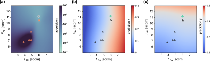
Two-dimensional plots of (a) acquisition values, (b) predicted x values, and (c) predicted y values as a function of FGa and FAs with six samples (triangles). The crosses represent the position of the minimum of acquisition value, selected as the next growth condition.
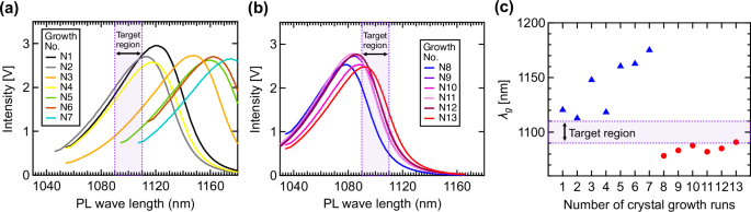
Following the PIBO, we grew the InGaAsP layer with the [{FGa, FAs} = {5.971, 11.2}], where the acquisition value is a minimum. The suggested FAs value is outside the FAs value range of the six preliminary data. Figure 5a, b shows the PL spectra of the six preliminary data (N1-N6 InGaAsP layers) and the N7 InGaAsP layer grown at [{FGa, FAs} = {5.971, 11.2}]. Figure 5c plots ({lambda }_{g}) as a function of the number of crystal growth runs. From the predictions based on six preliminary data that have only smaller ({lambda }_{g}) values than the target ({lambda }_{g}) of 1180 nm (Fig. 5a), the InGaAsP layer with a ({lambda }_{g}) of 1175 nm, which satisfies the termination requirement for optimization, was successfully obtained (Fig. 5b, c). Figure 6a, b shows θ-2θ scanned XRD patterns of the six preliminary data (N1-N6 InGaAsP) and the N7 InGaAsP layer grown at [{FGa, FAs} = {5.971, 11.2}]. Figure 6c shows the lattice mismatch as a function of the number of crystal growth runs. In the N1-N6 InGaAsP films [Fig. 6a], the (004) diffraction peaks of the InGaAsP layers appear at the lower or higher angles of the (004) peaks of the InP substrate, indicating that these films have lattice mismatches due to deviation from the target compositions. On the other hand, the (004) diffraction peak of the N7 InGaAsP film grown at [{FGa, FAs} = {5.971, 11.2}] [Fig. 6b] substantially overlaps the InP substrate peak and cannot be distinguished. This result indicates the InGaAsP layer has no lattice mismatch, satisfying the termination requirement for optimization [Fig. 6c]. The (scriptstyleleft({lambda }_{g},dright)) = (1175, 5.8688) of the N7 InGaAsP layer obtained from the above PL and XRD measurements corresponds to (left(x,yright)) = (0.192, 0.4176), which is very close to the first target composition (0.1953, 0.4247).
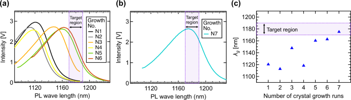
a PL spectra with six samples (N1-N6 InGaAsP layers). The λg values estimated from these PL measurements were used as a preliminary dataset for PIBO. b PL spectrum for the N7 InGaAsP layer. The λg value is within the target region of 1180(pm)10 nm. c λg as a function of the number of crystal growth runs.
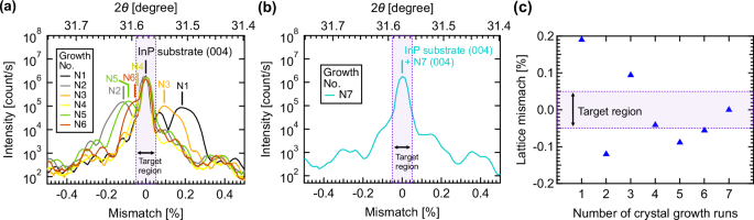
a XRD patterns of six samples (N1-N6 InGaAsP layers). The d values estimated from these XRD measurements were used as a preliminary dataset for PIBO. b XRD pattern for the N7 InGaAsP layer. The lattice mismatch is within the target region of 0(pm)0.05%. In (a, b), the color lines indicate the (004) diffractions of the InP substrate and InGaAsP layers. c Lattice mismatch as a function of the number of crystal growth runs.
As a subsequent optimization task, an InGaAsP layer having no lattice mismatch with a ({lambda }_{g}) of 1100 nm, which is smaller than the ({lambda }_{g}) range for the N1-N7 InGaAsP layers was fabricated by PIBO. The target (scriptstyleleft({lambda }_{g},dright)) = (1100, 5.8688) corresponds to (left(x,yright)) = (0.1404, 0.3065) (second target compositions). Here, the N1-N7 InGaAsP’s data obtained in the first optimization was used as the preliminary data for the PIBO. Similar to the previous optimization, exploration and exploitation in the growth parameter space according to the PIBO workflow led to synthesizing the InGaAsP layer with the target compositions. Fig. 7 shows the predicted results in the {FGa, FAs} growth parameter space for the data for the N1-N12 InGaAsP layers. In Fig. 7b, c, the white areas represent the regions where the predicted target x and y values are. Similar to the prediction results for the N1-N6 InGaAsP layers shown in Fig. 4, there is a monotonically increasing relationship of compositions to gas flow rates over the entire growth parameter space, with a tendency for the Ga (As) composition to be smaller (larger) than the In (P) composition in the As-rich (Ga-rich) region. The acquisition value reaches a minimum at {FGa, FAs} = {4.095, 6.869} [Fig. 7a]. As evidenced by the PL and XRD measurements shown in Figs. 8 and 9, the target InGaAsP layer satisfying the termination requirement has been synthesized under the growth condition. In the two tasks described above, InGaAsP layers with λg = 1180 nm and 1100 nm, i.e., values not in the range of the preliminary data, were synthesized using the PIBO in only one and six growth runs, respectively.
Two-dimensional plots of (a) acquisition values, (b) predicted x values, and (c) predicted y values as functions of FGa and FAs with 12 samples. The triangles and circles represent the preliminary data (N1-N7 InGaAsP layers) and the data (N8-N12 InGaAsP layers) obtained during the PIBO process, respectively. The crosses represent the position of the minimum of acquisition value, selected as the next growth condition.
a PL spectra for the N1-N7 InGaAsP layers. The λg values estimated from these PL measurements were used as a preliminary dataset for PIBO. b PL spectra for the N8-N13 InGaAsP layers. The λg value of the N13 InGaAsP layer is within the target region of 1100(pm)10 nm. c λg as a function of the number of crystal growth runs. In (c), the triangles and circles represent the preliminary data and the data obtained during the PIBO process.
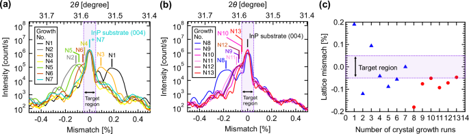
a XRD patterns for the N1-N7 InGaAsP layers. The d values estimated from these XRD measurements were used as a preliminary dataset for PIBO. b XRD patterns for the N8-N13 InGaAsP layers. The lattice mismatch of the N13 InGaAsP layer is within the target region of 0(pm)0.05%. In (a) and (b), the color lines indicate the (004) diffractions of the InP substrate and InGaAsP layers. c Lattice mismatch as a function of the number of crystal growth runs. In (c), the triangles and circles represent the preliminary data and the data obtained during the PIBO process, respectively.
Discussion
In laboratories and production sites around the world using MOCVD, rapid conditioning and composition adjustment are needed after equipment cleaning and equipment modification. In the future, if MOCVD vendors implement and commoditize the PIBO used in this study, compound semiconductors of any composition can be fabricated quickly by anyone, contributing to the productivity improvement of semiconductor manufacturing.
The PIBO implementation used in this study can generally be applied in the following situations and can be universally utilized for various material systems. When a known correlation exists between composition ratios and physical properties, such as Vegard’s law, the scaling issue in the parameter space can be avoided. Furthermore, when a relationship between experimental input parameters and composition or physical properties is known, as with the correlation between gas flow rate and composition, the PIBO framework presented in this study can be applied. As the simplest example, the PIBO model can also be applied to alloy semiconductors in general. Additionally, from the perspective of improving prediction accuracy through robust physics knowledge, when a phase diagram of a target material is available, it is possible to implement a strategy that the prediction model assigns undesired evaluation scores to regions where the target material is unlikely to be obtained. This would allow for a focused exploration of regions where the target material is more likely to be formed. Thus, we anticipate that this study will stimulate the development of PIBOs that integrate expert knowledge from various material systems.
In this study, we employed the simple assumption that there is a linear relationship between FGa (FAs) and Ga (As) composition since there is no established simulation model that can express the nonlinearity between gas flow rate and composition in compound semiconductors. The strength of our PIBO method is that deviations from the assumed linearity are predicted by the machine learning model as residual terms in Eqs. (4) and (5), allowing the growth results to be predicted without relying on individual simulation models. However, if a reliable simulation model specific to a material system exists, incorporating it as prior knowledge is expected to improve the prediction accuracy. For example, as reported in ref. 24, the CPM model is valid for 2D material growth, and the model can improve the uniformity and coverage of the growth. Additionally, ref. 25 reported the growth mechanism of h-BN films and revealed how the concentration of gas influences the uniformity of the grown layers. In the CVD growth of these 2D materials26,27, the morphology of the grown island depends on the flow rate of the precursor and rotation of the substrate, and these previous works can express its mechanism by the computational framework and preserve a match to the experimental result. Further development, improvement, and integration of both the machine learning prediction models and the conventional deductive simulation models are expected to further improve the prediction accuracy of the PIBO approach.
In summary, we developed a novel BO approach, PIBO, incorporating prior physics knowledge. Specifically, by incorporating Vegard’s law and the linear relationship between gas flow rate and composition into the BO method, we were able to synthesize III–V semiconductors with the desired band gap wavelengths and lattice constants that were outside of the region of growth conditions in the training data in a small number of growth runs. This result highlights the ability of PIBO to construct extrapolable machine learning models. We believe that this fusion of physics insights and machine learning will be crucial for developing physics-informed optimization models, with positive implications for high-throughput materials synthesis and autonomous synthesis.
Methods
Bayesian optimization for target values
Our goal is to build a layer with the desired ({lambda }_{{rm{g}}}^{* }) and ({d}^{* }). These targets are converted into equivalent representations of compositional ratios (left({x}^{* },{y}^{* }right)) by Vegard’s law. We sequentially try various pairs of (left({F}_{{rm{Ga}}},{F}_{{rm{As}}}right)) values to achieve the targets. The next setup (left({F}_{{rm{Ga}}}^{N+1},{F}_{{rm{As}}}^{N+1}right)) is determined from N past trials denoted by ({{mathcal{D}}}_{n}={left{left({F}_{{rm{Ga}}}^{n},{F}_{{rm{As}}}^{n},{x}^{n},{y}^{n}right)right}}_{n=1}^{N}).
First, we use the observations to build a prediction model in the form of Eqs. (4) and (5). Before fitting the GP component ({r}_{0}), we first estimate the linear regression coefficients ({a}_{0}) and ({b}_{0}). Specifically, we obtain the least squared estimators28:
where the sum ({sum }_{n}cdot) is taken over (n=1,ldots ,N). When ({widetilde{a}}_{0} ,>, 0), we set ({a}_{0}={widetilde{a}}_{0}) and ({b}_{0}={widetilde{b}}_{0}). Otherwise, ({a}_{0}=0) and (scriptstyle{b}_{0};=;frac{{sum }_{n}{x}^{n}}{N}). Note that these coefficients minimize the sum of squared residuals,
Thus, we expect that ({a}_{0}{F}_{{rm{Ga}}}+{b}_{0}) captures the increasing trend in x with regard to ({F}_{{rm{Ga}}}).
We use the GP to fit the residual ({z}_{0}^{n}:= {x}^{n}-{a}_{0}{F}_{{rm{Ga}}}^{n}-{b}_{0}) as a function of vector input of gas flows ({{boldsymbol{u}}}^{n}:= {left[{F}_{{rm{Ga}}}^{n},{F}_{{rm{As}}}^{n}right]}^{top })29(.) Here, (scriptstyle{cdot }^{top }) denotes the transpose operator. This model allows us to construct a predictive distribution of (x) values for unseen gas flows ({boldsymbol{u}}={left[{F}_{{rm{Ga}}},{F}_{{rm{As}}}right]}^{top }) given the estimated parameters ({a}_{0}) and ({b}_{0}). This predictive distribution is given as
Here, ({mathscr{N}}left(m,{s}^{2}right)) represents a normal distribution with mean (m) and variance ({s}^{2}). Note that the predictive mean has the ({a}_{0}{F}_{{rm{Ga}}}) term that increases with the input gas flow. The remaining terms (mu left({boldsymbol{u}}right)) and ({sigma }^{2}left({boldsymbol{u}}right)) are calculated using the standard GP prediction procedure, as follows30:
where ({{bf{k}}}_{1:N}) and ({{bf{z}}}_{1:N}) are N-dimensional vectors calculated from the data ({left{left({{boldsymbol{u}}}^{n},{z}_{0}^{n}right)right}}_{n=1}^{N}) and the kernel function (kleft(cdot ,cdot right)),
The kernel (kleft({boldsymbol{theta }},{{boldsymbol{theta }}}^{{boldsymbol{{prime} }}}right)) measures the similarity between ({boldsymbol{u}}) and ({{boldsymbol{u}}}^{{boldsymbol{{prime} }}}) and captures the covariance between corresponding ({z}_{0}) and ({z}_{0}^{{prime} }). We chose the radial basis function (RBF) kernel for our prediction model. The kernel is also used to calculate an (Ntimes N) matrix ({{bf{K}}}_{1:N}) in which the ith row and jth column element is (kleft({{boldsymbol{u}}}^{i},{{boldsymbol{u}}}^{j}right)). The prediction model for (y) is similarly constructed: the regression coefficients ({a}_{1}) and ({b}_{1}) are calculated from ({left{left({F}_{{rm{As}}}^{n},{y}^{n}right)right}}_{n=1}^{N}), and then GP is fitted to residuals.
Once the prediction model is constructed, the next experimental condition is derived using the idea that deviation (Delta ={left(x-{x}^{* }right)}^{2}+{left(y-{y}^{* }right)}^{2}) should be close to 0. The variable (Delta /{gamma }^{2}) approximately follows a noncentral chi-squared distribution30 with two degrees of freedom and noncentrality (C) and scaling ({{rm{gamma }}}^{2}) being
Let ({Q}_{{rm{NC}}}left({p;C},{gamma }^{2}right)) be the quantile function of the noncentral chi-squared distribution with the parameters above, where the cumulative probability is (0le ple 1). By the definition of the quantile function, we have
When we want (Delta) to be close to 0, the value of ({gamma }^{2}{Q}_{{rm{NC}}}left({p;C},{gamma }^{2}right)) is a good indicator with a certain (p). A small value of ({gamma }^{2}{Q}_{{rm{NC}}}left({p;C},{gamma }^{2}right)) means that the distribution of (Delta) is concentrated near zero. Remember that (C) and ({gamma }^{2}) depend on the input ({boldsymbol{u}}) via the GP prediction. Thus, we can specify the next ({{boldsymbol{u}}}^{N+1}:= left({F}_{{rm{Ga}}}^{N+1},{F}_{{rm{As}}}^{N+1}right)) by seeking the minimizer of ({gamma }^{2}{Q}_{{rm{NC}}}left({p;C},{gamma }^{2}right)). Our implementation used a constant (p=0.1). We may alternatively choose a decaying schedule, ({p}^{N}le {p}^{N-1}le ldots le {p}^{1}), as we observe more data (scriptstyle{left{left({F}_{{rm{Ga}}}^{n},{F}_{{rm{As}}}^{n},{x}^{n},{y}^{n}right)right}}_{n=1}^{N}). The decayed value of (p) emphasizes exploitation rather than exploration: a small (p) encourages small value of (scriptstyle{gamma }^{2}=frac{{sigma }_{x}^{2}left({boldsymbol{u}}right)+{sigma }_{y}^{2}left({boldsymbol{u}}right)}{2}) to minimize the product ({gamma }^{2}{Q}_{{rm{NC}}}left({p;C},{gamma }^{2}right)), meaning that there will be less uncertainty in terms of ({sigma }_{x}^{2}left({boldsymbol{u}}right),{sigma }_{y}^{2}left({boldsymbol{u}}right)) in the prediction by GP.
Note that in this paper we call ({gamma }^{2}{Q}_{{rm{NC}}}left({p;C},{gamma }^{2}right)) as the acquisition value and its minimum value is preferred for the next experimental configuration. This does not follow the common notation of BO literature, such as those in refs. 7,9, where the maximum acquisition is chosen for the next step. This is because our interest is how small distance we can make the experimental result from our target. The acquisition corresponds to an estimation of the distance.
MOCVD, PL, and X-ray diffraction setups
We used the MOCVD equipment manufactured by Veeco Corporation, and its model number is D180. The metal organic gas was vertically introduced to the InP substrates to realize uniform epitaxial growth. The InP substrates are rotating at 900 rpm during epitaxial growth. The growth temperature of all experiments was set to 650° C by applying a temperature monitoring system of D180. We used the n-type InP (001) substrates (2-inch size) commercially available from JX Nippon Mining & Metals Corporation. In our experiments, first, about 200-nm-thick InP buffer was grown on the substrate. Then, about 200-nm-thick InGaAsP layer was grown on the buffer layer, followed by the growth of about 65-nm-thick InP cap layer. We used the PL measurement equipment manufactured by Nanometrics Corporation, and its model number is RPM2000. The wavelength of the excitation light source is 532 nm. We employed X-ray diffraction equipment manufactured by Philips Corporation, and its model is X’pert. The X-ray wavelength is 1.54060 Å using Cu Kα for a line source, and germanium (220) X-ray monochromators are employed.


Responses