Physisorption-assistant optoelectronic synaptic transistors based on Ta2NiSe5/SnS2 heterojunction from ultraviolet to near-infrared

Introduction
Research in neuroscience and cognitive psychology has shown that the most essential way to acquire information about the outside world is visual perception1. Moreover, visual perception is a key technology for security surveillance, autonomous driving, face recognition, photoelectric tracking, and biomedical imaging. However, these application scenarios pose a significant challenge to the arithmetic power of visual perception. The traditional vision sensors utilize the von Neumann architecture, which presents challenges in boosting arithmetic capabilities and reducing power consumption due to the separation of the storage units and the computation units2,3. Fortunately, neuromorphic vision sensors offer a highly prospective solution for overcoming the arithmetic bottleneck in visual perception2,3,4,5,6,7,8,9,10,11. Neuromorphic vision computing dramatically breaks the arithmetic bottleneck by simplifying the raw data and optimizing data transfer between photodetectors and computation units12. More importantly, neuromorphic vision sensors hold substantial potential for mimicking the environment adaptation and in-memory sensing capability of human vision system13.
To improve information processing efficiency, reduce power consumption, and simplify the design in artificial systems, a highly compact all-in-one neuromorphic sensor has attracted increased attention because it can integrate visual perception, processing, and memory functionalities into one device14,15,16. Recently, the optoelectronic synaptic transistor has been attracting increasing attention as an all-in-one neuromorphic sensor because its three-terminal architecture can receive and read stimuli concurrently, accelerating signal processing17. Moreover, the gate electrode, as an additional third terminal, can effectively modulate the synaptic plasticity by regulating the conductance of the channel. The currently reported photoelectric synaptic transistors have demonstrated the in-memory sensing capability, but most of them can only operate at a specific wavelength or limited wavelength range1,14,16. This is because the photon energy decreases with the wavelength increasing, and the photoelectric conversion efficiency also decreases rapidly, resulting in the realization of non-volatile storage is also more difficult. A proposed solution involves employing the photogating effect to increase photoelectric conversion efficiency, especially for photons with longer wavelengths. The excellent photoelectric conversion efficiency is attributed to the remarkable photodetection gain: (G=frac{tau }{{t}_{{rm{L}}}}), where τ and tL are the lifetime and the transit time of the photocarrier, respectively18. Increasing carrier lifetime can increase both photodetection gain and data retention time, which partly solves the problem that optoelectronic synapses can no longer function under longer wavelength light stimulation.
The conventional method to increase the carrier lifetime is to block one type of carrier at the heterojunction interface to prolong the lifetime of another type of carrier, but this is far from enough. Another effective strategy is to prolong the lifetime further by taking advantage of the localized states caused by gas molecules’ physisorption in the air19. SnS2 is a two-dimensional material widely used for gas detection, due to its abundant intrinsic sulfur vacancies that can be used as gas adsorption sites and extend the carrier lifetime20. Besides, the intrinsic defects can effectively improve the performance of optoelectronic synapses by capturing and confining photogenerated carriers21,22. To further enhance the performance in NIR light, we use Ta2NiSe5 as an NIR absorber to improve the NIR adsorption of optoelectronic synaptic transistors. As a ternary chalcogenide with great potential in infrared detection, Ta2NiSe5 exhibits a direct narrow-band structure with 0.33 eV bandgap, which leads to an excellent NIR absorbance23. Accordingly, we use Ta2NiSe5 and SnS2 to form heterojunctions to explore the application of photonic synapses from ultraviolet (UV) to NIR.
In this work, we report physisorption-assistant Ta2NiSe5/SnS2 optoelectronic synaptic transistors which present in-memory sensing capability from UV to NIR regions due to significant PAPPC effect. We propose a strategy to greatly enhance the persistent photoconductivity (PPC) through adsorbing surface states and energy band engineering. Surprisingly, the Ta2NiSe5/SnS2 transistor exhibits not only an outstanding specific detectivity of 4.1 × 10¹⁴ Jones and an ultra-high external quantum efficiency of 1.7 × 10⁶% but also a superior photoresponsivity of 5.6 × 10³ A W−1 under 405 nm laser irradiation. Moreover, the device demonstrates a detectivity of 1.1 × 10¹² Jones and a photoresponsivity of 14.4 A W−1 in the NIR spectrum as well. Besides, the device can emulate diverse typical synaptic functions from 375 to 1310 nm. These functions are excitatory post-synaptic current (EPSC), the transitions from short-term plasticity (STP) to long-term plasticity (LTP), pair-pulse facilitation (PPF), emotion-controlled learning and memory process, learning behavior, and frequency-dependent learning properties. Furthermore, the classical Pavlovian associative learning is also simulated successfully, suggesting that our device can handle multiple input signals. Moreover, a proposed neuromorphic multi-spectral human visual system based on the Ta2NiSe5/SnS2 heterojunction mimics the color-cognitive perception and memory capabilities. Our strategy offers a viable approach for designing cutting-edge all-in-one neuromorphic sensors and developing multispectral neuromorphic computing vision. In addition, the applicability of optoelectronic synaptic transistors could be extended to multimodal (vision and olfactory) neuromorphic sensors for precise object recognition by employing the physisorption-assistant approaches.
Results
Fabrication and characterization of Ta2NiSe5/SnS2 heterojunction
Figure S1a displayed an optical microscope image of the Ta2NiSe5/SnS2 device. The layered Ta2NiSe5 and SnS2 flakes were obtained from their bulk materials through mechanical exfoliation and titanium/gold (20/80 nm) electrodes were made through ultraviolet photolithography and thermal evaporation. A detailed fabrication process of the Ta2NiSe5/SnS2 heterojunction can be found in the “Device fabrication” section. Next, Raman spectroscopy was employed to investigate phonon vibrations and interlayer coupling within Ta2NiSe5/SnS2 heterojunction, as shown in Fig. S1b. For pure Ta2NiSe5, there are seven distinct Raman peaks located at 95.7, 121.4, 147.8, 174, 189.4, 213.9, and 287.6 cm−1, which are related to the Ag vibration mode (blue line)24. For pure SnS2 flake, there is only one main peak located at 314.7 cm−1, which is associated with A1g vibration mode (yellow line)25. The Raman modes of both Ta2NiSe5 and SnS2 are observed in the spectra of the Ta2NiSe5/SnS2 overlapped region (red line), manifesting that the Ta2NiSe5/SnS2 heterojunction was effectively fabricated. Subsequently, atomic force microscopy (AFM) was employed to study the thickness and uniformity of the Ta2NiSe5/SnS2 heterojunction, as shown in Fig. S1c. Based on the AFM profiles depicted in Fig. S1d, the thicknesses of Ta2NiSe5 and SnS2 are 39.1 and 8.4 nm, indicating that the two materials are highly uniform. Last, we investigated the surface charge distribution of Ta2NiSe5 and SnS2 by Kelvin probe force microscopy (KPFM) measurement, as depicted in Fig. S1e, f. The KPFM measurements indicated that the Fermi level (EF) of SnS2 is 179.2 mV lower than that of Ta2NiSe5, which suggests a strong built-in electric field is formed.
Photoelectric characteristics of Ta2NiSe5/SnS2 device
To investigate the photoelectric characteristics of the Ta2NiSe5/SnS2 devices under constant light, the source-drain I–V curves were obtained at various laser powers 532 nm laser, as depicted in Fig. 1a. A clear distinction was observed in I–V curves with various laser powers, which indicated a strong photo-response. Then, the specific detectivity, external quantum efficiency, and responsivity of the Ta2NiSe5/SnS2 transistors were calculated at VDS = −3 V, as shown in Fig. S2. All the performance metrics decrease as the laser power increases, which presents trap-associated photoelectric performance26. The highest value of specific detectivity (D* = 2.50 × 10¹⁴ Jones), external quantum efficiency (EQE = 38810%), and responsivity (R = 166.3 A W−1) of the Ta2NiSe5/SnS2 device were obtained at the incident power of 2.1 nW, which presents excellent photoelectric characteristics under constant light. To study the transient photoelectricity response of the device, we measured the response of the Ta2NiSe5/SnS2 device under optical pulses of different powers of the 532 nm laser at the condition of VDS = −3 V. Figure 1b depicts that the photocurrent of Ta2NiSe5/SnS2 device did not drop immediately to initial current level but still maintain consistent for a specific duration after light excitation, which can be attributed to PPC effect27. Furthermore, we found that the decay process can be modulated by applying multiple light pulses, which offers the potential for diverse forms of synaptic plasticity5,28. A similar phenomenon can be observed in the broadband from UV to NIR range, as shown in Fig. S3. The statistical robustness of the photoresponse was discussed in Supplementary Note 1, which is crucial for the application of neuromorphic machine vision. The four parallel tests of the three devices exhibit comparable responsivity, thereby confirming the reproducibility of responsivity data. Thus, our devices have great potential for realizing wide-band optoelectronic synaptic applications.

a Output curves (IDS–VDS) in the dark and under illumination with different powers. The incident light is at 532 nm wavelength and VG = 0 V. b Time-resolved photoresponse of the Ta2NiSe5/SnS2 device at VDS = −3 V. The incident light is at 532 nm wavelength and VG = 0 V. The gray part represents the light pulses applied to Ta2NiSe5/SnS2 device. c Transfer curves (IDS–VG) in dark and under illumination with different power. The incident light is at 532 nm wavelength and VDS = −1 V. d Band diagrams of the junction under light illumination. e Band diagrams of the junction after light illumination. f Photocurrents at VDS = −3 V under lasers from 375 to 1310 nm with various light intensities. All test results are from four parallel tests, data points and plot lines are the mean of the four results, error bars and error bands represent the standard deviation of the four results
Next, we studied the transfer curves of the Ta2NiSe5/SnS2 transistor to explore the mechanism of PPC generation. Firstly, we examined the transfer characteristic of the Ta2NiSe5/SnS2 transistor in the non-illuminated state and compared it with the transfer characteristic of the pure Ta2NiSe5 transistor and the pure SnS2 transistor, as depicted in the inset of Fig. 1c. The characterization and fabrication details of pure Ta2NiSe5 and pure SnS2 devices can be seen in Fig. S6 and the “Device fabrication” section. The thickness of the pure Ta2NiSe5 device and pure SnS2 device are 30 and 13 nm respectively, which is basically consistent with the two materials in the Ta2NiSe5/SnS2 device. In the inset of Fig. 1c, when VG changes within the range of -30 V to 30 V, the current of Ta2NiSe5 material remains at the level of 10-5, indicating that the impact of gate voltage on the carrier density of Ta2NiSe5 material is negligible. However, the current of the SnS2 device changes drastically from 10-12 to 10-9, spanning 3 orders of magnitude, which shows that the gate voltage can significantly change the carrier density of the SnS2 material and the majority of carriers of the SnS2 material are electrons. Interestingly, the changing trend of the transfer curve of the Ta2NiSe5/SnS2 device is consistent with that of the SnS2 device, which shows that the gate voltage primarily changes the electron density in the channel of the Ta2NiSe5/SnS2 device. It is noted that the current dynamic range of the Ta2NiSe5/SnS2 device is almost two orders of magnitude larger than the SnS2 device, which proves that our device exhibits excellent gate control performance. Secondly, we studied the effect of light on the transfer characteristic of the Ta2NiSe5/SnS2 device by irradiating the device with 532 nm light of different powers, as shown in Fig. 1c. The transfer curves of the Ta2NiSe5/SnS2 device gradually shifted to the left and the threshold voltage changes significantly with increasing light power, which suggests that the main component of the photocurrent was photogenerated electrons while the majority of photogenerated holes trapped in the heterojunction18,29,30. This phenomenon suggests an asymmetric transport behavior of photogenerated carriers in the device, possibly causing the generation of the PPC.
Accordingly, we illustrate this PPC phenomenon due to the asymmetric transport of photogenerated carriers. According to currently reported studies of two materials (Ta2NiSe523,26,31, SnS225,32,33) and the KPFM measurements (Fig. S1e, f), a type II heterojunction is formed as shown in Fig. S7. At reverse bias (VDS = −3 V), the energy band structure of the Ta2NiSe5/SnS2 device will tilt, causing electrons to flow from SnS2 to Ta2NiSe5 and holes to flow in the opposite direction, as shown in Fig. 1d. With light illumination, the photogenerated carriers generated by SnS2 are transported to the electrodes under the electric field. However, among photogenerated carriers generated by Ta2NiSe5, only photogenerated electrons can be transported, while photogenerated holes will be blocked by the interfacial potential barrier. The trapped photogenerated holes create a photogating effect, causing the electrons to undergo multiple cycles in the heterojunction channel, resulting in a significant gain. After light illumination, the blocked photogenerated holes can still induce numerous nonequilibrium electrons to generate a continuously decaying current, as shown in Fig. 1e. Moreover, O2 and H2O molecules will be absorbed on the surface of the channel of SnS2 in the Ta2NiSe5/SnS2 device. The sites of the O2 and H2O molecules may induce additional localized states to prolong the lifetime of the photogenerated electrons34,35, which extremely enhances the PPC phenomenon, as shown in Fig. 1d, e. To verify the role of physisorption assistance in PPC, we compared the time-resolved photoresponse in air and vacuum, as shown in Fig. S8a, b. Under physisorption assistance, the PPC is effectively enhanced and the relaxation time of the decay process (determine the memory time) was boosted by an order of magnitude, which is consistent with our theoretical explanation. It is noted that the photoelectric detection performance (except for the response speed) was almost unaffected by physisorption, as shown in Fig. S8c. Since we deliberately block the carriers of Ta2NiSe5, which can absorb the NIR photons, the energy band structure of the heterojunction can produce a significant PAPPC effect even under NIR illumination, thus broadening synaptic function to the NIR band.
Subsequently, we investigated the photocurrent of the device under illumination from UV to NIR light to validate our theoretical explanations, as shown in Fig. S9–11. We summarized the specific detectivity and responsivity of the transistors at 375–1550 nm, in the inset of Fig. 1f. The responsivity and detectivity of our device have two peaks at 405 and 980 nm. The peak responsivity reaches 5.6 × 10³ A W−1 (14.4 A W−1) and the peak detectivity reaches 4.1 × 10¹⁴ Jones (1.1 × 10¹² Jones) at 405 nm (980 nm). The reasonable explanation is that the SnS2 (Ta2NiSe5) materials have an absorption peak at 405 nm (980 nm), which is consistent with previous research reports21,36. In addition, by employing a power-law relationship to fit the power-dependent photocurrents, Iph∝Pα (Fig. 1f), the α in the longer wavelength lights (635, 980, and 1550 nm) is significantly inferior to those in the shorter wavelength lights (375, 405, and 532 nm). In the previous studies, the α represents the loss in photocarrier transport37,38. The lesser the value of α, the larger the loss of photocarriers in transport. Considering the cutoff wavelength of SnS2 (λc = 563 nm), the longer wavelength lights (635, 980, and 1550 nm) represent the photocurrent generated by Ta2NiSe5. The low α index indicates there exists a massive carrier loss in photocarriers generated by Ta2NiSe5, which is associated with asymmetric transport of photogenerated carriers that the vast majority of photogenerated holes from Ta2NiSe5 are blocked by interfacial potential barriers.
Light tunable synaptic behaviors in Ta2NiSe5/SnS2 device
Figure 2a illustrates a model of the human visual system. When light enters the eye, light signals are transformed into electrical signals and transmit preprocessed electrical signals into the cerebral cortex by transmitting neurons to visual recognition and perception. When a retinal cell receives a light pulse signal input, the information is stored as an excitatory pulse in the form of exponential decay in post-synaptic current (PSC). This means that all information decays naturally, and only the information that is frequently used is retained, making this a breakthrough in the bottleneck of the von Neumann computing system. Inspired by the retina, the Ta2NiSe5/SnS2 device can perform the neuromorphic function of the photoreceptor cell.
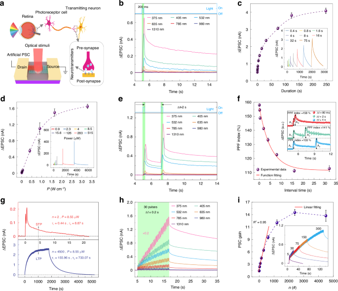
Light tunable synaptic behaviors in Ta2NiSe5/SnS2 device. a Schematic of the entire biological visual system. b An EPSC of Ta2NiSe5/SnS2 device triggered by an optical pulse. The duration of the optical pulses is 200 ms. The power of the optical pulses from 375 to 1310 nm are 0.15 μW, 0.36 μW, 0.26 μW, 1.89 μW, 5.66 μW, 21.05 μW, and 1.19 mW. c Dependence of the EPSC triggered by an optical pulse on the pulse duration. The duration and power of the optical pulses are 200 ms and 13.26 μW. Error bars represent the standard deviation obtained from four times independent tests of Ta2NiSe5/SnS2 device. d Dependence of the EPSC triggered by an optical pulse on the power of the pulses. The duration of the optical pulses is 200 ms. Error bars represent the standard deviation obtained from four times independent tests of Ta2NiSe5/SnS2 device. e EPSC of Ta2NiSe5/SnS2 device triggered by a pair of optical pulses with a duration of 200 ms. The interval time(△t) between the two pulses is 2 s. The power of the optical pulses from 375 to 1310 nm are 0.15 μW, 0.79 μW, 1.73 μW, 13.26 μW, 6.19 μW, 421 μW, and 1.19 mW. f Dependence of the PPF index (defined as A2/A1) on △t. The red solid line results from the fitting with an exponential function. g The dependence of transition from STP to LTP on the quantity of the optical pulses. The duration and interval time of the optical pulses are 200 and 200 ms, respectively. h EPSC of Ta2NiSe5/SnS2 device triggered by 30 pulses. The time interval between the pulses is 200 ms. The power of the optical pulses from 375 to 1310 nm are 0.15 μW, 0.02 μW, 0.51 μW, 2.3 μW, 43.04 μW, 219 μW, and 857.77 μW. i Dependence of PSC gain on the quantity of the optical pulses. Error bars represent the standard deviation obtained from four times independent tests
To explore the device’s capability in detecting and recording optical signals, we irradiated the device with a single light pulse of 375–1310 nm with a duration of 200 ms. Figure 2b illustrates the typical EPSC response observed in the Ta2NiSe5/SnS2 device. After light stimuli, the Ta2NiSe5/SnS2 device responds to light signals of various wavelengths with distinct EPSC values and memory time. Therefore, our device has the potential to perceive and distinguish the optical signals from 375 to 1310 nm. More details about the EPSC in NIR can be seen in Fig. S12a. The decrease in EPSC peak value was observed to be significantly correlated with the increase in wavelength, attributed to the weakening of the photogate effect, which will be discussed in Supplementary Note 2. Taking the synaptic behavior at 635 nm as an example, we next discuss the modulation of EPSC by changing light pulse power and duration. In Fig. 2c, as the pulse duration increases, the EPSC peak value also increases, reaching a saturation value of 4.08 nA when the pulse duration is 250 s. This phenomenon closely resembles the variability of EPSC in a biological synapse within a neural system39. A similar phenomenon can be observed in NIR, as shown in Fig. S12b. As the optical pulse intensity increases, the maximum value of EPSC also increases, as shown in Fig. 2d. We further investigate the multilevel storage capabilities of our synaptic device under the programming operation of single pulses with various light powers in 635 nm, as shown in Fig. S15. The results show that multilevel discernable current states could be written by light pulses with various light powers and the retention time was higher than 50 s. The above experimental results demonstrate that the Ta2NiSe5/SnS2 transistor has the potential to detect and store multiple light information, such as wavelength, power, and duration of light pulses.
Pair-pulse facilitation (PPF) is one of the prominent characteristics of STP, where consecutive presynaptic stimuli lead to an enhancement of the postsynaptic signal; it is essential to receive and process visual information in real-time40,41. In Fig. 2e, the EPSC resulting from a pair of optical spikes is illustrated. The spike duration is 200 ms, and the inter-spike interval (△t) is 2 s. It is evident that the EPSC evoked by the second optical spike (A2) exceeds that evoked by the first optical spike (A1) in the range of 375–1310 nm, demonstrating the well-established phenomenon of PPF. More details about the PPF in NIR can be seen in Fig. S12c. This phenomenon arises from the fact that the photo-generated carriers from the initial optical pulse do not undergo complete recombination upon stimulation by the subsequent optical pulse. Taking the synaptic behavior at 635 nm as an example, we next investigated the ratio A2 to A1 (i.e., PPF index) depending on △t, as shown in Fig. 2f. The PPF can be quantified by the ratio of the two EPSCs, that is, PPF index = (A2/A1) × 100%. The maximum PPF index of 158% is obtained when the △t is 80 ms. The PPF index exponentially decays as △t increases. A similar phenomenon can be observed in NIR, as shown in Fig. S12d, e. Such observation is consistent with the information process in a biological synapse, and the high PPF index is crucial for high-precision decoding and processing of visual information5. The above experimental results demonstrate that the Ta2NiSe5/SnS2 device has the potential to preprocess the multispectral information. A detailed comparison between Ta2NiSe5/SnS2 devices and other optoelectronic synaptic devices is presented in Table S1. Our devices possess a distinct advantage in the combined performance of operating wavelength range, PPF index, and power consumption.
In biological systems, the transition from short-term potentiation (STP) to long-term potentiation (LTP) can be induced through repetitive pulsed stimulation, leading to a continuous enhancement of synaptic strength42; it is essential for biological memory and learning. Figure 2g shows the transition from STP to LTP by changing the number of light pulses. It is noted that as the number of optical pulses increases from 2 to 4500, the peak value of the EPSC increases dramatically from 0.21 to 2.6 nA and the retention time (i.e., the time when the EPSC peak decays from 90% to 10% of its initial value) increases from 11.29 to 1299.51 s, which indicates that the effectiveness of learning and memory time can be modulated by learning times. To further investigate the transition from STP to LTP, we fit the decay process of EPSC with the double-exponential decay equation:
where relaxation time constant τ1 and τ2 correspond to two decay mechanisms with different rates: fast band-to-band transition (τ1) and slow carrier de-trapping (τ2), of which the slow process with relaxation time constant τ2 plays the decisive role in determining the forgetting rate18,40. The decay process can be well-fitted by using the double exponential decay function, as shown in Fig. S16. The time constants for the decay of STP and LTP in the Ta2NiSe5/SnS2 device are 8.87 and 733.07 s, respectively (Fig. 2g). This suggests that the rate of forgetting can be significantly modulated by repetitive learning. Subsequently, we investigated the transition from STP to LTP under optical stimulation from 375 to 1310 nm. Figure 2h depicts the EPSC triggered by 30 optical pulses of 375-1310 nm with a duration of 200 ms, demonstrating the emulation of the typical transition from STP to LTP of retinal cells during repeated light stimulations. The time interval (△t) between these two optical spikes is 200 ms. More details about the transition from STP to LTP in NIR can be seen in Fig. S12f. The value of EPSC increased significantly with the increase of pulse number during 30 consecutive light pulses, as shown in Fig. 2h. This is attributed to the PAPPC effect due to the large number of photogenerated carriers produced after repeated stimulation with light pulses. The above experimental results demonstrate that the Ta2NiSe5/SnS2 device has the potential to learn and remember multispectral information.
We further studied the key parameters of the LTP which have a major impact on the accuracy of hardware artificial neural networks43. Firstly, we investigated the dependence of the EPSC gain (determined as An/A1) on the number of optical spikes which is related to the contrast in neuromorphic imaging and preprocessing28, as shown in Fig. 2i. When the pulse number is less than 300, the EPSC gain increases linearly with the pulse number; when the number of pulses is greater than 300, the dependence of the EPSC gain on the number of pulses deviates from linearity and eventually saturates. Next, we studied the dynamic range of the Ta2NiSe5/SnS2 device, as shown in Fig. S17a. The dynamic range is defined by the following equation:
where PSCmax is steady state PSC after 30th pulse, and PSCmin is steady PSC after 1st pulse1. After 30 light pulses, the device exhibits a dynamic range of 10.43 dB, which indicates the potential to contain multiple conductance states and is crucial for high-precision neuromorphic computing44. The synaptic performance of the Ta2NiSe5/SnS2 device can be further adjusted to manipulate the PAPPC effect by modifying the gas environment, which was discussed in Supplementary Note 3. Subsequently, we investigated the non-linearity of the Ta2NiSe5/SnS2 device, as shown in Fig. S17b. The formula provided below is utilized to model the LTP process of the synapse45:
where GLTP and Gmin denote the current level under the light pulse and the initial state, respectively. P and Pmax represent the pulse number and the maximum number, while B and A are constants that require to be fitted. A is influenced by the nonlinearity of weight update and can be either positive or negative. B is a function of A within the range of Gmin and P. Generally, as A approaches 0, the curve’s linearity improves28. The nonlinearity of our device, measured at 26.57, is a critical factor for its application in neuromorphic computing. The above experimental results demonstrate that the Ta2NiSe5/SnS2 device has the potential in hardware artificial neural networks.
The tunable long-term plasticity of the optoelectronic synaptic transistors
It is widely accepted that moods can influence the processes of learning and forgetting46. Because the gate electrode can effectively regulate the conductance of the channel, the Ta2NiSe5/SnS2 device has great potential for simulating the effects of emotion on learning. We simulated the learning progress with 30 continuous light pulses and simulated the forgetting progress with the decay of EPSC after 30 continuous light pulses. Figure 3a shows the EPSC triggered by 30 optical pulses under various gate voltages at 635 nm laser. As the gate voltage varies from −10 to 5 V, the maximum value of the EPSC increases as the gate voltage increases. We can define the person has a neutral mood when Vg = 0 V. For Vg < 0 V and Vg > 0 V, the person has a negative mood and a positive mood, respectively. It is noted that the learning results are forgotten more quickly (slowly) for a negative (positive) mood, which is consistent with the mood’s effect on human learning.
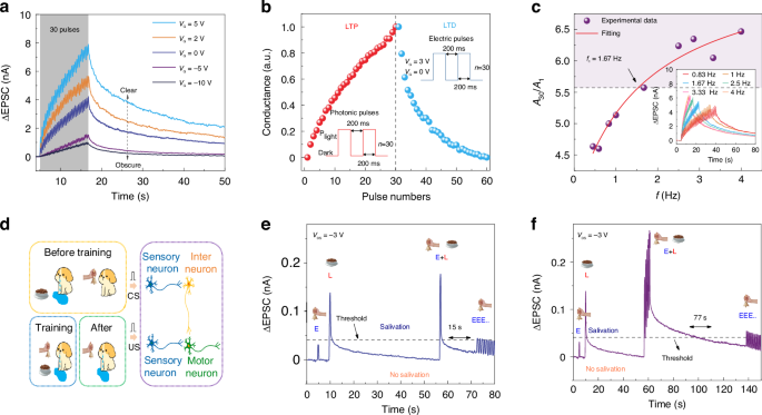
a Dependence of the EPSC triggered by 30 optical pulses on various back-gate voltages. The bias voltage (VDS), wavelength, duration, and power of the optical pulses are −3 V, 635 nm, 200 ms, and 13.26 μW. b LTP/LTD characteristics. Light and voltage pulses for LTP and LTD are depicted in the figures. Photonic pulses conditions of the Ta2NiSe5/SnS2 device are 635 nm, 13.26 μW power, 200 ms width. c Dependence of the gain of EPSC (A30/A1) on the pulse frequency. The wavelength, duration, and power of the optical pulses are 635 nm, 200 ms, and 13.26 μW. d Schematic illustration of Pavlov’s dog experiment and the neural circuit of associative learning. Classical Pavlovian conditioning under e one and f five training (E + L)
It has been proposed that long-term potentiation (LTP) and long-term depression (LTD) are crucial for the memories encoding47. LTP and LTD of the Ta2NiSe5/SnS2 device are updated by optical and electrical pulses, respectively, as shown in Fig. 3b. The LTP and LTD characteristics of the Ta2NiSe5/SnS2 device depend on the pulse number of light pulses and gate-voltage pulses, separately. Figure S21a illustrates the use of light spikes and gate-voltage pulses (Vg = 3 V) to control synaptic function, transitioning from LTP to LTD. This involves potentiation after 30 consecutive optical stimuli, followed by depression induced by 30 gate-voltage pulses. After 30 optical pulses, the current increases significantly due to the accumulation of photogenerated holes, as shown in Fig. S21b. When positive gate voltage pulses are applied to the Ta2NiSe5/SnS2 device, the interfacial barrier of the heterojunction decreases, and the blocked photogenerated holes are released under the electric field, as shown in Fig. S21c. After 30 gate voltage pulses, the Ta2NiSe5/SnS2 device current returns to its initial value due to the release of photogenerated holes, as shown in Fig. S21d.
LTP of the Ta2NiSe5/SnS2 device can be modulated by the frequency (f) of the optical pulses, as shown in Fig. 3c. The frequency of the optical pulses (f) is defined by the following equation: f = t2/(t1 + t2), where t1 is the duration of light pulses, t2 is the interval of light pulses. The gain of the EPSC after 30 optical pulses (A30/A1) increases with the increase of the pulse frequency, which presents a high-pass filtering characteristic. The high-pass filter is able to effectively block signals with a low frequency below the cut-off value while permitting high-frequency signals to pass through, which is essential for preprocessing images in the human retina48. To further investigate the cutoff frequency of our device, we fit the frequency-dependence of EPSC gain with the sigmoidal function: (g(f)=({a}_{1}-{a}_{2})/(1+{(f/{f}_{c})}^{p})+{a}_{2}), where p is the order of the function, fc is the cut-off frequency, a1 and a2 are the initial and final amplitude48,49. The gain curve can be best fitted with p = 1. The fitting results in a value of 1.67 Hz for fc. The similarity to the high-pass filtering characteristic of biological synapses indicates that the Ta2NiSe5/SnS2 device holds promise as a high-pass filter for image preprocessing, including image sharpening48.
Due to the tunability and long-term plasticity of the optoelectronic synaptic transistors, the Ta2NiSe5/SnS2 device has the potential to simulate associative learning between two physical inputs, such as the Pavlovian conditioning, as shown in Fig. 3d. The dog will instinctively secrete saliva when it sees food. We call the behavior of secreting saliva as the unconditional reflex (UR) and call the behavior of seeing food as the unconditional stimulus (US). The dog will not secrete saliva when it hears a bell. We call the behavior of hearing a bell as the neutral stimulus (NS). If we deliberately ring the bell while the dog is eating, the dog associates hearing the bell with having food to eat. After training, the dog will associate US with NS and will salivate even if it only hears a bell. We call the behavior of the dog secreting saliva when it hears a bell as the conditional reflex (CR)5,48.
To mimic this Pavlovian associative learning, we defined the application of a gate voltage pulse (+0.1 V, 200 ms) as a bell stimulus, the application of a light pulse (13.26 μW, 200 ms) as a food stimulus, and the simultaneous application of both a gate voltage pulse and a light pulse as one training to make the dog believes that there exists a connection between food stimulation and ringing stimulation, as shown in Fig. 3e. The drain current is defined as the terminal that detects the CR and UR output signals. The threshold current (Ith = 41 pA) for the salivary response was marked with a black dashed line in Fig. 3e, f. When we apply the gate voltage pulse (NS), only a weak current pulse (31.5 pA) is generated in the channel, which does not reach the threshold. That is, applying only a bell stimulus (NS) does not make a puppy salivate (UR). When we applied the light pulse as food stimulation (US), the current rapidly increased to 145 pA, significantly above the threshold, causing the puppy to salivate (UR). However, the current rapidly decreased and fell below the threshold after the light pulse was withdrawn. When we applied both a gate voltage pulse and a light pulse as food and ringing stimuli (US + NS), the current rapidly increased to 177 pA and exceeded the threshold causing the puppy to salivate, suggesting the link between food and ringing was established. After a training session and the current dropped to about 20 pA, if multiple gate voltage pulses are applied again, only the first three gate voltage pulses trigger currents above the threshold, which means that the training can only provisionally associate NS with CS to induce CR. This phenomenon is similar to the biological nervous system. In order to eliminate redundant information from the nervous system, CRs that are not trained regularly will fade away. With repeated training, it is possible to maintain the CR for a longer time. After 5 training sessions and the current dropped to about 20 pA, CR will be strengthened and the triggered current is above the threshold even after 19 gate voltage pulses, as shown in Fig. 3f. Interestingly, even at 980 nm, our device is able to achieve this Pavlovian association learning, as shown in Fig. S22. This suggests that our device can realize the basic function of synapses even in the NIR band.
Simulation of the behavior of the human visual system
Usually, humans acquire new knowledge through three processes: initial learning, partial forgetting, and relearning. During relearning, human can recover their memory to the original level with only a small amount of learning and the stability is greatly enhanced48. We used light pulses to simulate the process of learning and re-learning and used a dark-state environment to simulate the natural decay process of learning memory (Fig. 4a). During the first learning process, the current increased to 480 pA, then after a 17.57 s forgetting process, the current decreased to 175 pA. During the relearning process, the current recovered to 480 pA with 15 pulses, which indicates a progressive learning efficiency in the relearning process. Similarly, undergoing the same forgetting process, the current only decays to 190 pA, which reflects the ability to make the memory effect significantly stronger through learning and reviewing, which is similar to the Ebbinghaus forgetting curve in brain memory40.
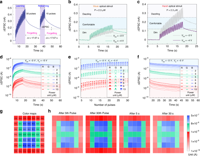
a The “learning-forgetting-relearning” process triggered by multiple light pulses. b, c Simulation of the light adaptive behavior of human visual system in 635 nm wavelength application scenario. d EPSC variations of Ta2NiSe5/SnS2 device under RGB-light pulses (635, 532, and 405 nm) with various light power from 2 to 13 μW. RGB pulse conditions: 200 ms width and 200 ms interval. e EPSC distribution depending on the number of RGB-light pulses extracted from (d). f The decay of the EPSC after 30 RGB-light pulses extracted from (d). g We used the RGB-light information shown in the figure for single-point scanning imaging. For example, “R-6” represents red light pulses (635 nm) with 6 μW. The duration, interval, and quantity of all the optical are 200 ms, 200 ms, and 30, respectively. h 2D contour map of PSCs measured from Ta2NiSe5/SnS2 device at different pulses and retention time conditions. All measurements were performed at a drain voltage of −3 V and a gate voltage of −5 V
A key function in the human visual system is adaptation to light power, which allows the human visual system to process visual information in environments with drastic changes in light power5. When exposed to dim (or harsh) light, the human eye will initially feel uncomfortable and progressively become able to see them following visual adaptation. If the light is too dim, the device can amplify the photocurrent by increasing the bias voltage, as shown in Fig. 4b. If the light is too harsh, the device can reduce the background noise by reducing the bias voltage, as shown in Fig. 4c. Hence, the simple-structure Ta2NiSe5/SnS2 device shows promising potential to be employed as an artificial pupil in artificial visual systems.
Next, we explored the potential of the Ta2NiSe5/SnS2 device as a retinal cell for color recognition applications. In the retina, the short, middle, and long wavelength-sensitive cone photoreceptors are responsible for acquiring the visible light information to produce color vision50. Inspired by the retina, we used RGB-light pulses (R:635 nm for red color; G: 532 nm for green color; B: 405 nm for blue color) with various light intensities from 2 to 13 μW to illuminate the Ta2NiSe5/SnS2 device to mimic the color recognition behavior of the retinal cell. The numbers of red color, green color, and blue color pulses are all 30. As shown in Fig. 4d, it is noted that the EPSC currents corresponding to the three different colors (red, green, and blue) were distinguished. To further explore the color-discrimination capability, we studied whether there is color overlap for EPSC currents. Specifically, the largest EPSC value of red color should be lower than the least EPSC value of green color and blue color in each state1,50. Similarly, the largest EPSC value of green color should be lower than the least EPSC value of blue color in each state. If the above two points are met at the same time, we believe that there is no color overlap in EPSC current. In Fig. 4e, we found that from the 5th to 30th RGB-light pulses, the EPSC of R-light is always lower than that of the G-light and B-light. Similarly, the EPSC of the G-light is always lower than that of the B-light. In Fig. 4f, there is no color overlap in the EPSC currents corresponding to the three different colors after 30 RGB-light pulses with various intensities within 43.2 s. As a result, the Ta2NiSe5/SnS2 device is able to effectively discriminate the RGB light in the range of 213 μW without mixing color. Subsequently, we measured the RGB imaging of the device using single-point scanning.
Accordingly, we performed a neuromorphic imaging experiment by single-point scanning. Specifically, we performed 49 independent repetitions of light stimulation on the Ta2NiSe5/SnS2 device to obtain a 7 × 7-pixel color picture. Each light stimulation consisted of 30 continuous light pulses. Take the first light stimulation as an example, we applied the color information of “R-6” in the first row and first column of the color map (Fig. 4g) to the device in the form of 30 continuous 635 nm light pulses at 6.3 μW. We recorded the PSC change of the Ta2NiSe5/SnS2 device and did not perform the next light stimulation until the PSC returned to its initial value. After 49 independent repetitions of the experiment, we achieve the neuromorphic imaging, as shown in Fig. 4h. We found that the Ta2NiSe5/SnS2 device achieved color discrimination of RGB-light with different intensities after the 5th pulse. As the pulse number increased, the color difference became more obvious, which indicates the ability of color recognition can be strengthened through multiple learning. Besides, we found that the Ta2NiSe5/SnS2 device can accurately remember the color information in the 30 s. Our devices show great potential for the recognition, preprocessing, and memory of color information.
Discussion
To summarize, we have demonstrated the physisorption-assistant optoelectronic synaptic transistors with a prominent performance in recognition, preprocessing, and memory of multispectral information. We propose an effective strategy to greatly enhance the performance of optoelectronic synaptic transistors through physisorption surface state and energy band engineering. Under this strategy, our device exhibits a high specific detectivity of 4.1 × 10¹⁴ Jones (1.1 × 10¹² Jones), an ultra-high external quantum efficiency of 1.7 × 10⁶% (1.8 × 10³%), and responsivity of 5.6 × 10³ A W−1 (14.4 A W−1) in visible (NIR) light. Due to the PAPPC effect, our device is capable of emulating typical synaptic functions across a broad spectrum ranging from UV to NIR, including EPSC, PPF, and the conversion from STM to LTM. The synaptic plasticity of the device can be modulated by gate voltage pulses, resulting in distinguishable, multi-level nonvolatile memory-based electronic synaptic behavior, which is eventually able to mimic modulation of emotions on visual learning and memory processes and optical write-electro-erase. Furthermore, with the synergistic action of light and gate voltage, our optoelectronic synaptic transistor endowed the emulation of Pavlov’s associative learning. Moreover, we developed a simplified human visual system to simulate color-cognitive perception and memory functions. Our approach offers a route for creating advanced all-in-one neuromorphic sensors and developing neuromorphic computing vision. In the future, gas adsorption-assisted optoelectronic synaptic devices are expected to handle different types of stimuli and are becoming an important trend in sensing technology aiming at better recognition accuracy and robustness.
Materials and methods
Device fabrication
The Ta2NiSe5 and SnS2 flakes were mechanically exfoliated from bulk single crystals purchased from HQ Graphene Ltd and Six Carbon Technology Ltd. by using scotch tape and transferred to Polydimethylsiloxane (PDMS) film (METATEST Corporation, China). The Ta2NiSe5 flake was transferred as the bottom material of the heterojunction onto the pre-cleaned Si/SiO2 (285 nm) substrate by PDMS using a high-precision 2D material transfer platform (METAT-EST Corporation, China, E1-T). Next, SnS2 flakes were successfully transferred as the top material of the heterojunction to the Ta2NiSe5 side using the same method. The metal electrodes with a spacing of 20 μm were pattered by UV-lithography. Then, titanium (Ti)/gold (Au) contacts were deposited with a thickness of 20/80 nm by thermal evaporation. The vdWs heterojunction will be annealed at 200 °C under N2 gas for 20 min to ensure closer stacking at the interface. Subsequently, we used the same process to make the pure Ta2NiSe5 device and the pure SnS2 device.
Characterization of Ta2NiSe5/SnS2 device
The morphology of each material was examined with the use of the Optical Microscope (BX51, OLMPUS). The Raman spectra were acquired using a WITec micro-Raman system (532 nm laser). AFM and KPFM images of the Ta2NiSe5/SnS2 heterojunction were collected by Asylum Research Cypher S (Oxford).
Optoelectrical measurement
The electrical tests were carried out under typical environmental conditions at standard room temperature. A semiconductor parameter analyzer (Keithley 4200) was employed to characterize the static behaviors of the optoelectronic synaptic transistors. The illumination conditions were provided by different lasers: IR (785, 980, 1310, and 1550 nm) and RGB-light (405, 532, and 635 nm) and ultraviolet (375 nm). The temporal response and synaptic characteristics of the optoelectronic synaptic transistors were characterized by a semiconductor parameter analyzer (METATEST Corporation, China, Metatest E2).
Synaptic test in gas environment: The synaptic test in gas environment were carried out in the probe station. The gas sensing performance of the sensor was measured by monitoring the variation of the current (Tektronix, USA, Keithley 2636B) in the air and the target gas. The three mass flow controllers (Seven-star, China, CS-200A) were used to vary the O2 amount from 50% to 100% by changing the flow ratio between O2 and N2.
Supporting information
Detailed information about characterization of Ta2NiSe5/SnS2 heterojunction, photoelectric characteristics of Ta2NiSe5/SnS2 device, synaptic characteristics of Ta2NiSe5/SnS2 device.
Responses