Programmable quantum circuits in a large-scale photonic waveguide array

Introduction
Implementing a universal set of quantum gates is a crucial requirement for a physical system in the standard framework of quantum computing1. Linear optical circuits offer a versatile platform to perform quantum computing tasks2 and have evolved from free space optics to integrated photonic circuits3. An essential requirement for such technology is the ability to generate controllable and high-visibility quantum interference between single photons with tunable beam splitters4. This can be achieved with Mach-Zehnder interferometers (MZIs) consisting of a phase shifter and two balanced directional couplers (DCs).
In large-scale integrated systems, MZIs equipped with extra phase shifters5 play a fundamental role in manipulating quantum states6,7,8. In addition, large-scale optical networks consisting of several electrically tunable MZIs and phase shifters9,10, are required for realizing quantum photonic processors able to perform any arbitrary linear optics operations on quantum states of light11,12. Beyond quantum computing, programmable photonic circuits13 are a key component in numerous other emerging technologies, including quantum transport simulations14, microwave photonics15 and optical neural networks16.
The schemes based on MZIs suffer from bend losses proportional to the depth of the circuit, and they are not robust against fabrication errors17,18,19,20. Furthermore, the bending radii are typically significantly longer than the coupling length6, meaning the circuit area is dominated by routing waveguides that do not contribute to the logical operation. Photonic waveguide arrays (WA) have been proposed as an alternative that overcomes the aforementioned challenges. WA are periodic structures composed of optical waveguides evanescently coupled to each other21. Since the first demonstration of a two-photon continuous quantum walk on a WA with 21 waveguides22, there have been numerous advancements in the field of quantum applications using WAs, ranging from topologically protected quantum state generation23,24,25 to quantum state processing26,27,28. Additionally, theoretical and experimental work has explored the feasibility of using waveguide arrays for implementing 1 and 2-qubit gates29,30,31. These structures can also simulate a wide range of condensed matter physics effects32,33,34,35,36 as well as offer the possibility of directly implementing tri-diagonal Hamiltonians, in a direct (analog) instead of digital way. Recently, we have provided a mathematical proof that cascaded reconfigurable waveguide arrays (RWA) can implement any unitary matrix, even under realistic constraints such as limited control and finite array size37, and demonstrated an RWA based on the lithium niobate photonics platform, implementing multiple condensed matter physics models38.
In this paper, we demonstrate the implementation of reconfigurable single-qubit gates on an 11-waveguide electro-optically reconfigurable waveguide array (11-RWA), by decoupling pairs of waveguides and implementing subcircuits in the form of tunable DCs within the array. Additionally, we tune the degree of quantum interference with a maximum visibility of 0.962 ± 0.013 in the subcircuit. Finally, we demonstrate the possibility of using the chip to decouple multiple pairs of waveguides to control multiple single qubits in parallel. Our technology enables large-scale photonic quantum information processing based on reconfigurable continuously-coupled waveguide arrays, providing a platform with improved fabrication error tolerance and reduced bending-loss17,19,20, and direct access to and control of the Hamiltonian terms and evolution38.
Results
Reconfigurable waveguide arrays via electro-optic control
The 11-RWA used in this work is fabricated on x-cut lithium niobate, with a designed continuously-coupled region of 24 mm. The reconfigurability of the device is enabled by creating electric fields across the cross-section of the array via electrodes positioned on the top of the waveguides. Further details about the device can be found in the Methods.
An ideal 11-RWA device shown in Fig. 1a can be modeled by the voltage-dependent tri-diagonal Hamiltonian21
where the propagation constant βn and coupling constants Cn,n+1 between adjacent waveguides (WG) (n indicate the waveguide label) can be controlled via electric field generated by (overrightarrow{v}=left({V}_{1},{V}_{2},..{V}_{22}right)) from 22 electrodes, which changes the refractive index of the material via the Pockels effect. The unitary transformation of the device is given by
where L is the effective coupling length of the device.

a The 11-RWA has 11 waveguides (black), which implements a voltage-dependent unitary ({U}_{11times 11}(overrightarrow{v})), programmed via electric fields applied to the electrodes (orange). b Electrode configuration to implement the experiments in this work, the cross-section of the RWA, and the schematic of subcircuits DC1,2 and DC8,9. By decoupling optical modes 1 and 2 from the other modes of the circuit, WG1 and WG2 act as an independent coupled system DC1,2. Path encoding is used in this work, i.e., (left|0rightrangle=begin{bmatrix}1&0end{bmatrix}^T) is encoded as a photon in optical mode 1, (left|1rightrangle=begin{bmatrix}0&1end{bmatrix}^T) is encoded as a photon in optical mode 2. c By decoupling and post-selection, the single photon input states (leftvert {psi }_{1}rightrangle) and (leftvert {psi }_{2}rightrangle) are processed independently by two 2 × 2 unitaries, effectively implementing two single-qubit quantum gate operations.
We used a fiber-coupled polarized 808 nm laser diode for classical characterization of the device and the setup used to control the device is illustrated in the Methods. The voltage corresponds to the amplitude of the non-biased square pulse. Further details can be found in the Supplementary materials.
In practice, this model does not apply accurately to a real device. Due to the limited fabrication quality, the performance of certain electrodes was suboptimal. The best-performing electrodes were selected for this experiment to demonstrate the potential of our protocol in isolating specific parts of the circuit. To control the device, a model-based machine learning approach39,40, or model-free approaches can be used. In this paper, we obtain the controlling voltages by using a model-free approach in which measurement-based lookup maps are built for different configurations and then those maps are used to search for the required control voltages satisfying given criteria (such as a target reflectivity with minimum leakage). Details can be found in the Supplementary materials.
Subcircuit control in an RWA
One of the key requirements for implementing universal multiport interferometers9,10 using RWAs, is the capability of splitting an RWA into decoupled subcircuits as shown in Fig. 1 (i.e. decoupling a subset of the waveguides from the rest, and being able to control that subset independently), as well as implementing arbitrary 2 × 2 unitary operations.
To decouple a subcircuit, the coupling constants between the boundary waveguides of the target subcircuit and the rest of the RWA need to be reduced to zero. This will result in a structure of three subcircuits with the Hamiltonian reduced to a block diagonal matrix of the form H11×11 = H1 ⊕ H2 ⊕ H3. Consequently, the resulting unitary will also be a block diagonal of the form U11×11 = U1 ⊕ U2 ⊕ U3. Here, we show the decoupling of a 2 × 2 subcircuit which provides the basis for qubit operations as well as the main building block of higher-dimensional unitary decomposition methods. A general 2 × 2 unitary can be represented as:
where UDC is the unitary of a tunable DC with η indicating its reflectivity and Rz is the unitary transformation of a phase shifter with ϕ defining the phase. In our technology, both η and ϕ are voltage-dependent, and, in this work, we restrict our measurements to η.
In practice, achieving a coupling constant of zero might be difficult with a limited voltage range. This results in imperfect decoupling and the leakage of optical power from a target subcircuit to the rest of the waveguides. The leakage can be quantified using the definition:
where Pi is the percentage normalized measured output power at WGi, the index k is the subcircuit index of interest and N is the total number of waveguides. In this paper, we demonstrate the decoupling of the subcircuit consisting of WG1 and WG2(as shown in Fig. 1). Since this is an edge subcircuit, the RWA will be split into two subcircuits rather than three. We empirically decreased the value of C2,3 in Eq (1) by applying a voltage of 7 V to electrode 4 (V4 = 7 V) on the RWA. Specifically, for light input in WG1, the leakage is reduced from 63% to 33%, and for light input in WG2, it is reduced from 81% to 35%, compared to the scenario where 0 is applied to electrode 4 (V4 = 0 V, see Fig. 1b and Supplementary materials). We varied the propagation constant β1 of WG1 by sweeping the V1 from -10 to 10 V (see Fig. 1b and Supplementary materials) to control the reflectivity η of DC1,2, to obtained to realize a subcircuit that implements a tunable DC within the 11-RWA.
Figure 2a reports a simulation of light propagating through the RWA when injected into WG1 and WG2, with the decoupling voltage applied to electrode 4. In the simulations, the Hamiltonian evolves over the device length, and probability distributions are computed using the model in reference38, with no voltage amplitude limitations. These results align well with the measured reflectivity shown in Fig. 2b. With the decoupling voltage restricted to avoid physical damage to the device, part of the light can leak to the rest of the RWA during the propagation. A simulation of the relationship between leakage and decoupling voltage can be found in Supplementary materials. In Fig. 2b, we report the experimental measurements of the voltage-dependent output power from the 11-RWA with light input in WG1 and WG2, respectively.
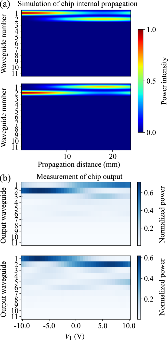
a Numerical simulations of the propagation of light inside the chip for input waveguides 1 (top) and 2 (bottom), where DC1,2 is decoupled and V1 = 0 V. b Experimentally measured optical output power of the RWA for input waveguides 1 (top) and 2 (bottom), as a function of the voltage on electrode 1 based on the configuration for in Fig. 1c.
Reconfigurable quantum interference
The capability of generating high-visibility two-photon quantum interference is crucial for photonic quantum technologies41,42. We performed reconfigurable quantum interference43 experiments within the subcircuit DC1,2, providing a proof-of-concept for continuously-coupled integrated photonic systems. Photon pairs at wavelength 807.5 nm generated by a spontaneous parametric down-conversion source (see Methods) are launched into WG1 and WG2 with the input state (frac{1}{sqrt{2}}(leftvert 01rightrangle +leftvert 10rightrangle )) as shown in Fig. 1a (encoding scheme is explained in the Fig. 1 caption). We measured the two-photon coincidence rate while scanning a physical delay line of one of the photon beams at different reflectivity of DC1,2. Ideally, when η=0.5, two photons come out from the same waveguide with the output state (frac{1}{sqrt{2}}(leftvert 00rightrangle +{e}^{ipsi }leftvert 11rightrangle )) at a unity probability due to ‘photon bunching’ effect44, which gives zero coincidence counts between two waveguide outputs.
The visibility is a measure of the contrast of the HOM ‘dip’ in quantum interference experiments. Each experiment is done by measuring the two-photon coincidence counts as a function of relative delay between two-photon paths at a fixed voltage configuration as shown in the insets in Fig. 3 (blue data points). A Gaussian function with a linear term is used to fit the measurement results to extract the visibility45 (shown as the orange lines). Details about the fitting procedure are provided in the Supplementary materials. The insets show two examples of such an experiment at two different voltages corresponding to two different reflectivities. The visibility at reflectivity η = 0.496 (V1 = 0.5 V) is (bar{V}=0.962pm 0.013). The visibility at reflectivity η = 0.897 (V1 = 4.5 V) is (bar{V}=0.265pm 0.058). The reflectivity η as a function of voltage is calculated from the power measurements in Fig. 2b and is shown as the red dashed line. The procedure is then repeated to sweep the visibility measurement (shown as the purple data points) over a voltage range that corresponds to the reflectivities ranging from 0.5 to 1. Finally, the ideal visibility as a function of voltage is calculated from the reflectivity at the same voltage and shown as the purple dashed line. The calculations can be found in the Supplementary materials. The results show that the measured visibility is consistent with the ideal calculated visibility.
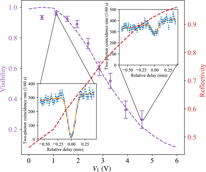
The insets show two-photon interference experiments, performed at two different voltages that are applied to electrode 1, where the blue points represent the measured two-photon coincidence rate integrated over 60 s as a function of the relative delay, and the orange line is the fitting. The error bars represent the standard deviation based on the assumption of Poissonian photon statistics. The left inset shows a high-visibility configuration, while the right inset shows a low-visibility one. The visibility is estimated from the fitting and plotted as a function of the voltage shown as the purple points. The error bars of the visibility are based on the calculations detailed in the Supplementary Materials. The red line is the measured reflectivity as a function of voltage of this configuration based on Fig. 2b. The purple dashed line shows the theoretical visibility versus voltage calculated from the reflectivity at the same voltage.
Parallel quantum gates
Controlling multi-qubit systems is crucial to advanced quantum technologies46. We demonstrate this capability by running single-qubit operations on two independent qubits simultaneously8 within the RWA. We implement a second subcircuit DC8,9 as shown in Figs. 1c and 4a with the electrode configuration shown in Fig. 1b. Decoupling voltages are applied on V13 and V20 and V16 = −4.5 V is used to shift the reflectivity curve to gain a larger tunable reflectivity range.
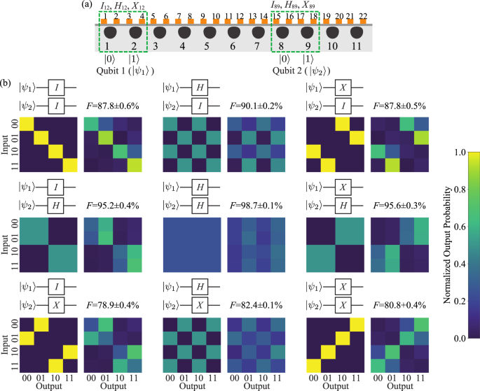
a Schematic of the experiment implementing two tunable subcircuits. By selecting the reflectivity, single qubit gates such as the identity I, Hadamard H, or Pauli X are realized for two path-encoded qubits (leftvert {psi }_{1}rightrangle) and (leftvert {psi }_{2}rightrangle). b Single-qubit gates (I, H, and X gate) are implemented by controlling DC1,2 and DC8,9, with two balanced laser inputs in parallel. For each operation, we show the ideal map (left) and the experimentally measured map (right). We also report the post-selected average fidelity F over all input states.
To showcase the capability of implementing the single-qubit gates in parallel on DC1,2 and DC8,9, we launched two balanced laser beams into two subcircuits separately by splitting the laser into two beams with a 50/50 808 nm fiber-coupled beam splitter and measure the output power for 4 different input combinations. We built a lookup map by varying both tuning electrodes at the same time (see supplementary material). The reflectivity required for implementing single-qubit X, H, and I gates are η = 0, 0.5, and 1. We found the corresponding voltages based on linear fitting of the reflectivity curves of each DC based on the measured lookup map to run parallel quantum gates. In Fig. 4b, we report the ideal and measured truth tables and the fidelity for all combinations of two single-qubit gates based on post-selected results by ignoring the leakage.
The post-selected average fidelity (over input states (iin {0,1,2,3}equiv {leftvert 00rightrangle ,leftvert 01rightrangle ,leftvert 10rightrangle ,leftvert 11rightrangle })) for the parallel operation is given by (F=frac{1}{4}mathop{sum }nolimits_{i = 1}^{4}{F}_{i}), where ({F}_{i}=mathop{sum }nolimits_{j = 1}^{4}sqrt{{P}_{i,j}^{T}{P}_{i,j}^{M}}) is the fidelity between the target and measured output power distributions for the input state i, and the summation is over the output states (jin {0,1,2,3}equiv {leftvert 00rightrangle ,leftvert 01rightrangle ,leftvert 10rightrangle ,leftvert 11rightrangle }). The normalized power distribution is calculated as ({P}_{i,j}^{M}=frac{{M}_{I(j)}}{{sum }_{kin 1,2,8,9}{M}_{k}}), where I(j): {0, 1, 2, 3} → {1, 2, 8, 9} is the index mapping between state encoding j and the waveguide index, and Mk is the measured power at output waveguide k.
The post-selected average fidelity of all parallel quantum gates experiments is 88.5%. They are relatively good except in some cases when I and X gates on DC8,9 are involved. This is because the lookup maps, created based on limited control, do not fully cover the space of the unitaries that can be implemented by the device and lack the solutions for achieving high-fidelity I and X gates on DC8,9.
The overall average fidelity across the 11 waveguides in all parallel quantum gate experiments is 74%, approximately ~14.5% lower than the post-selected average, accounting for the leakage caused by the limited controllability. The overall fidelity f is calculated as (f=frac{1}{4}mathop{sum }nolimits_{i = 1}^{4}{f}_{i}), where ({f}_{i}=mathop{sum }nolimits_{m = 1}^{11}sqrt{{p}_{i,m}^{T}{p}_{i,m}^{M}}) is the fidelity between the target and measured output power distributions for the input state i across the entire device. The normalized power distribution is calculated as ({p}_{i,m}^{M}=frac{{M}_{i(m)}}{mathop{sum }nolimits_{m = 1}^{11}{M}_{i(m)}}).
Noting that here only a small subset of the available control electrodes were used, our simulations (see Supplementary materials) suggest that increasing the number of electrodes and expanding the voltage range can enhance controllability and consequently improve the overall fidelity. Nevertheless, while further optimization is necessary to find better control voltages, our results demonstrate the proof of concept.
Discussion
In this paper, we have demonstrated reconfigurable quantum interference and parallel single-qubit operations on a large-scale RWA, a major advancement over previous photonic WAs that were static35,36 or not directly and fully controllable47. While the thermo-optic effect is currently the prevailing approach for reconfiguring photonic circuits, it cannot be employed to construct a fully controllable waveguide array device, due to the diffusive propagation of the thermo-optic effect along the material causing cross talk48. In contrast, here we used the electric field, which is confined within the material due to the shielding effect from neighboring electrodes, enabling stable and precise control in electro-optic devices49.
Our protocol shows clear potential for isolating subcircuits in various configurations. However, fabrication imperfections affected the performance of several electrodes, limiting the number of waveguide pairs that could be tested experimentally. Future efforts should focus on improving the fabrication methods to ensure more reliable electrode performance, allowing for broader testing of different waveguide pair combinations.
In addition to improving fabrication, there are two main directions for enhancing global control over the entire chip. First, extending the device length enhances electro-optical reconfigurability, while increasing the number of active control electrodes and expanding the voltage range reduces leakage, broadens the reflectivity range, and improves overall fidelity, as shown in the supplementary material. Experimental validation of this more complex setup is still needed, and future research should explore a wider variety of waveguide pairs to deepen understanding of the device’s control capabilities. Second, while a single section of the RWA implements a limited set of N × N unitary transformations, cascading multiple devices enables the realization of arbitrary N × N unitaries. This has been proven theoretically and numerically in37, even under constraints such as limited control and finite array size. For instance, approximately 20 sections of the RWA can achieve 11-dimensional Haar random unitaries with an average fidelity exceeding 99.9%. Therefore, either enhanced global control or cascading additional sections is expected to support the operation of circuits with n > 2 waveguides.
The measurement-based lookup map method used in this work addresses the challenge of having an accurate mathematical model for the fabricated device. In this paper, we focused on building maps for reflectivity and leakage using power measurements. The method can be extended to settings where the phase information is also available. This will allow better characterization of the leakage and light power crosstalk between subcircuits. The phase information can be acquired with either classical light only39,50,51 or quantum light via HOM measurements52,53,54. In this work, we fixed the voltage steps applied to two electrodes, creating a uniform resolution over the range of the map. As larger circuits and improved control require an increased number of control electrodes, the complexity of building lookup tables also grows. To address this computational challenge, non-uniform or adaptive sampling can be used to optimize resolution efficiently. Additionally, there are machine learning methods (such as Bayesian optimization55) that automate the process of building the lookup maps and the optimization simultaneously.
To expand the device’s capabilities for quantum computing applications, implementing a two-qubit CNOT gate is essential. There are several potential pathways to achieve this. One approach is to directly locate the target unitary of a two-qubit gate in lookup maps by spanning its controlling parameters or using other machine learning methods39,40,55. Another option is to design a device that naturally implements the CNOT gate without any applied control30,31. However, this approach faces controllability issues when adding tunability. Additionally, the CNOT gate can be decomposed into three sections, with each section implementing single-qubit gates exclusively56. This can be achieved by cascading three sections of RWAs, with each RWA needing to implement single-qubit gates.
To further improve the performance and scalability of such devices, efforts need to be put into device design and fabrication. For example, the newly developed z-cut thin film lithium niobate platform57 allows different electrode patterns and reduced footprint while offering the capability of on-chip single-photon sources58,59 and detectors60. The modeling method used in this work is based on38, which assumes a real-valued tridiagonal Hamiltonian and linear voltage-Hamiltonian dependence. While this ideal model provides useful insights, it has been shown to deviate from the actual device behavior40. Incorporating FDTD propagation simulations61 with electric field simulations could yield a more accurate representation of the device. However, this approach requires significant computational resources and is more feasible for devices with smaller dimensions.
The results presented here highlight the potential of such a device as a fundamental building block for arbitrary unitary transformations17,20 or as an alternative approach to implementing the discrete scheme9,10, offering advantages in reduced bending loss (see supplementary materials) and robustness against fabrication errors. Other potential applications besides the ones presented in this paper include high-dimensional quantum computing62, and topological quantum computation63. It is worth noting that WAs have been extensively used in demonstrating topological effects. These effects can be leveraged to generate topologically protected quantum states and build topologically robust quantum gates25,27,64,65, offering an alternative approach to implementing universal gate sets. Our results point towards building integrated linear optical quantum circuits in a continuously-coupled way of manipulating photon states with potential applications in quantum metrology, quantum simulations66, and quantum information processing.
In summary, this work is the first proof-of-principle demonstration of using continuously-coupled waveguide arrays, instead of networks of beamsplitters (Reck or Clements scheme), as a new architecture for photonic quantum computing. The presented device enables controllable operations on subcircuits through the application of electrode voltage for channel decoupling. Our achievement of a high-visibility (96%) two-photon quantum interference within a subarray is a crucial step towards implementing quantum circuits with this technology. Additionally, we successfully demonstrated parallel control of single-qubit gates on two subcircuits. This work establishes a substantial connection between quantum information science and photonic engineering, showcasing the potential of precise control of RWAs for future quantum technologies. These results open up new avenues for further research in the design, fabrication, and control of such devices.
Methods
Experimental setup
A polarized 808 nm laser and multi-channel fiber-coupled high-speed optical power meter with oscilloscopes are used for classical characterizations. A multi-channel AWG is used to generate pulses that are applied to electrodes to program the 11-RWA. The power distribution of the static classical characterization of the RWA for each input waveguide is extracted from the power intensity measured by a CCD camera at the output facet of the RWA. In the parallel gate measurements, the 808 nm laser is split into two beams via a 50/50 808 nm fiber-coupled beam splitter.
A schematic of the quantum interference measurements setup is shown in Fig. 5. A type 1 free space spontaneous parametric down-conversion (SPDC) single photon source (purple dashed frame) and single photon counting modules (SPCMs) are used to generate and detect photon pairs. The SPCMs are from Excelitas Technologies (SPCM-800-12-FC) with a measured dark count rate ~ 30/s. Each channel has a counting rate ~ 8000/s with an expected accidental rate of less than 1 per minute. The transmission loss is primarily attributed to fiber-to-chip coupling, resulting from a mismatch between fiber and waveguide modes. The total transmission loss was measured at 9.8 dB (90%), and the device has a total length of 62 mm. From numerical simulations, we estimate an 80% overlap between the mode supported by the waveguide and the one of an optical fiber, and negligible metal-induced propagation loss due to the presence of the electrodes. Given the measured transmission of our device, this corresponds to a propagation loss coefficient of 1.3 dB/cm. Note that this value is an upper bound to the actual propagation loss coefficient, as this estimation does not take into account other loss factors that might contribute to a reduced fiber-to-chip coupling efficiency. A 1mm BiBO crystal is pumped by a 403.75 nm, 80 mW continuous laser. Two generated photons with an opening angle of 3∘ are separated by two prism mirrors, pass through a narrow band filter with a Full width at half maximum (FWHM) of 3.1 nm and are then coupled into two PMFs. One of the polarization-maintaining fibers (PMFs) is mounted on the motor-controlled stage, which enables a tunable delay. Photon polarization is rotated from horizontal to vertical before photons are coupled into the PMFs. Single-mode fibers (SMFs) are used to couple the chip outputs. The integration time of single-photon experiments is 60 s.
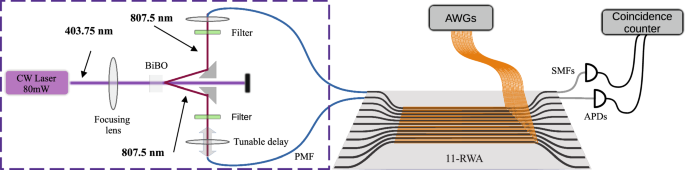
A spontaneous parametric down-conversion (SPDC) single photon source (in purple dashed frame) is used to prepare single photon states. A multi-channel AWG output is connected to the electrodes of the 11-RWA via a ribbon cable. Avalanche photodiodes used to detect photons are connected to a coincidence counter.
Device fabrication
The 11-RWA is fabricated using annealed and reverse proton exchange technology with x-cut bulk lithium niobate. The designed waveguide mode has a diameter of 5 μm and is separated by a distance of 5 μm. The gold electrode has a width of 2.5 μm and is separated by a distance of 2.5 μm38. A 200 nm silicon dioxide buffer layer is placed between the lithium niobate and gold electrodes. Further design and fabrication methods can be found in40,67,68.
Controlling pulses
Applying controlling voltages on electrodes causes DC drift of LiNbO3 due to electric charge accumulation, which results in a drift of optical output states of the chip69. 100 Hz modulated non-biased square pulses generated by AWGs are used to stabilize the optical output states70. Each electrode is connected to a channel of arbitrary waveform generators (AWGs) independently. An external trigger is used to synchronize multiple AWGs. Voltage-dependent output power distributions in classical characterizations are taken from an average of 20 periods post-selected parts of the square pulse. In quantum interference measurements, the square pulses are continuously applied until a sufficient integration of two-photon coincidence counts is achieved. Long-term drift over tens of hours was measured to be negligible by continuously applying this control method and measuring the chip output states. Additionally, classical light characterization was conducted on different days from the HOM experiments, confirming the repeatability of the experiments.


Responses