Promises and challenges of indoor photovoltaics

Introduction
The Internet of Things (IoT) enables energy-efficient buildings by optimizing control of systems such as heating, ventilation and lighting1, which is crucial for minimizing global energy consumption and greenhouse gas emissions2. The IoT market is rapidly growing3, with an estimated integration of more than 40 billion devices into the IoT ecosystem by 2027 (ref. 4). Wireless IoT nodes have a lifespan of over 10 years but an average primary battery life of approximately 2 years5, necessitating frequent battery replacements or recharging. In 2025, an estimated 78 million batteries from IoT devices will be discarded daily5, presenting economic and environmental challenges due to the greenhouse gas footprint and the costs associated with battery disposal3,5.
Half of new IoT set-ups are installed indoors3,6, where abundant indoor ambient light (artificial and natural6) has higher energy density than other forms of ambient energy1. The intensity of indoor light levels varies greatly (Fig. 1), but indoor light sources are ubiquitously and predictably available and can be harvested by indoor photovoltaics (IPVs) to power IoT nodes. For example, IoT sensors often operate under indoor lighting conditions with illuminances ranging from 50 to 400 lux, sufficient for powering devices such as smart watches, asset trackers and building-automation sensors, which typically require 50–150 µW or ~60 µW cm−2 incident power7. Under bright spots of 1,000-lux illuminance typical in supermarkets, optical power densities of approximately 300 µW cm−2 are available. IPV cells of >10 cm2 area delivering ~30% power conversion efficiency can generate a few milliwatts of power at 1,000 lux (ref. 8), sufficient to operate many IoT devices such as electronic shelf labels3. IPV could reduce the frequency of battery replacements or remove batteries entirely in IoT devices.

Indoor photovoltaics (IPV)-powered devices will have different lighting intensities depending on their location. Incident light levels can be over 1,000 lux by windows with direct sunlight, or as low as around 50 lux on the ceiling in a corner. Materials for IPV applications, and the control electronics for IPV devices, need to be designed to take this variation of light intensity into account and maintain stable operations over device lifetimes.
Some IPV technologies are well established, with several approaching commercialization. Various IPV technologies surpass industry-standard hydrogenated amorphous silicon (a-Si:H)9. For instance, dye-sensitized solar cells (DSSCs), organic photovoltaics (OPVs) and lead halide perovskites (LHPs) have all reached an indoor power conversion efficiency (PCEi) range of 30–45%8,10,11. At 200 lux, 10-cm2 IPV modules using III–V semiconductors have a power output of 21.8 µW cm−2 (ref. 12), which is sufficient to replace tens of AAA batteries per device over their multiyear lifespan.
In this Review, we discuss the status and challenges of existing and emerging materials for IPVs, focusing on compounds derived from low-toxicity halides and chalcogenides. We calculate and analyse their radiative-limited and spectroscopic-limited maximum efficiencies (SLMEs) and propose standardized frameworks for reliable IPV performance measurements and characterization13. We cover advances in scaling up IPV technologies, including principles for designing high-efficiency modules, and integration of IPVs with smart electronics to power autonomous IoT devices. Finally, we examine the sustainability concerns and manufacturing challenges of IPVs, including the recycling of certain critical materials and components, and technoeconomic and policy barriers to the commercialization of emerging IPV technologies.
Devices and materials
Indoor light intensities vary, so IPVs must generate sufficient power and voltage at various (even low) light levels, and their performance should decrease as little as possible on decreasing the illuminance. The spectral wavelength of the light source can also vary with time of day, as natural and artificial lighting mix. In this section, the performance requirements for IPVs, established IPV technologies and emerging technologies are discussed.
IPV performance requirements
IPV performance should be assessed in illuminance (lux) rather than power density (W cm−2), as indoor lighting tends to be characterized by the spectral response of the human eye rather than absolute radiometric units. Light intensities typically chosen to characterize IPVs usually vary from 200 to 1,000 lux, which is reasonable given that indoor lighting standards focus primarily on human task-oriented activities14. However, the light source available to IPV devices can often reduce to as low as 50 lux (for example, when placed in the shadow of an object)15,16.
Indoor environments in buildings with numerous windows receive a combination of diffused natural lighting and artificial lighting, resulting in changes in the spectral distribution of available ambient light throughout the day — from bright natural light in the morning to wholly artificial light at midnight15. The spectrum is not entirely predictable, and it varies with the environment and changes in the intensity of diffused natural light15. Materials with bandgap values in the 1.7–1.8-eV range are well suited for harvesting this mixed ambient light15,17. A wider bandgap of 1.9–2.0 eV is optimally suited for harvesting 1,000-lux artificial lighting18,19,20. For instance, an absorber with a bandgap of 1.9 eV can achieve a maximum open-circuit voltage (VOC) of 1.4 eV at 1,000-lux artificial lighting. An ideal IPV technology should include absorbers with high absorption coefficients and optimized morphology. It should be processable in a sustainable manner, maintain low manufacturing costs and ensure reliable high performance under different light intensities and spectra.
For IPV materials, the ideal PCEi should be at least 30% to produce ~1 mW of power under 1,000-lux illumination with a reasonable device area of ~10 cm2. The VOC should also be as high as possible, to reduce the number of devices that need to be connected in series to meet the required operating voltage for IoT electronics. For example, a target value of 2.65 V is needed for a typical battery-less multisensory IoT platform20. Many emerging technologies, such as DSSCs, OPVs and LHPs, have achieved a VOC greater than 1 V, with LHPs reaching the highest value of 1.25 V among these technologies21. Along with a wide bandgap, low bulk and interfacial trap recombinations are highly desired for maximizing VOC under indoor lighting conditions, owing to the low densities of photogenerated charge carriers at low incident light intensities21,22,23,24. A maximum short-circuit current density (JSC) of ~120–140 µA cm−2 is predicted under 1,000-lux indoor illumination25. Producing devices with JSC values close to their theoretical limits requires optimizing the thickness and photoresponse spectrum of the absorber material25,26,27.
Established IPV technologies
IPV absorbers need to be efficient and stable, made of non-toxic and non-regulated elements (for example, compliant with the EU Restriction of Hazardous Substances (RoHS) directive 2002/95/EC)28, and able to be manufactured cost-effectively over large areas. The current industry-standard material, a-Si:H, meets the requirements for cost-effective manufacturability at scale, RoHS-compliance and stability, with reported PCEi values up to 21% (but typically 4.4–9.2% under typical indoor light spectra)29. Higher PCEi values have been achieved by IPV devices using III–V semiconductors, even under low illuminance, reaching 37.5% at 100 lux (ref. 30). The losses in VOC and fill factor (FF) are only 78 mV and 2.1%, respectively, as the intensity decreases from 1,000 to 100 lux (ref. 30) (Fig. 2a,b). Such low losses can be attributed to the high shunt resistance, of the order of 106 Ω cm2 (ref. 30). However, III–V technologies are typically limited by their high fabrication costs. Cadmium telluride (CdTe) and copper indium gallium sulfide (CIGS) thin films are more cost effective to make3. Yet CIGS-based IPVs have a low shunt resistance of 6.5 × 10⁴ Ω cm2 and therefore display a severe drop in VOC (ΔVOC = 156 mV) and FF (ΔFF = 31.7%) from 1,000 to 100 lux (Fig. 2a,b), resulting in a PCEi of only 4.5% at 100 lux.
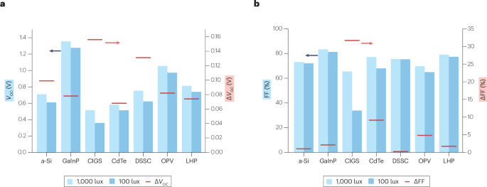
a, Open-circuit voltage (VOC) of various photovoltaic cells and modules, obtained from commercial suppliers and recognized labs, under 1,000-lux and 100-lux lighting from white light-emitting diodes. b, Fill factor (FF) values of cells and module. The solid horizontal lines in panels a and b indicate the differences in the VOC and FF, respectively. Data (obtained from ref. 30), including areas and suppliers of each device, are available in Supplementary Table 2. a-Si, amorphous silicon; CdTe, cadmium telluride; CIGS, copper indium gallium sulfide; DSSC, dye-sensitized solar cell; GaInP, gallium indium phosphide (III–V); LHP, lead halide perovskite; OPV, organic photovoltaics.
A high shunt resistance of ≥106 Ω cm2 and minimized bulk recombination are the key requirements for minimizing the PCEi losses for any IPV device, particularly under low light intensities of ≤200 lux (refs. 31,32,33). Severe FF and VOC losses occur under low light intensities in materials with low shunt resistances, because too low a shunt resistance causes a high leakage current, which remains constant with light intensity, whereas the photocurrent decreases as light intensity drops30,31,32,33. The lower the resistance, the greater the FF loss. High-quality, thick absorber layers with optimized morphologies can lead to high shunt resistance in devices, as non-uniformities in the absorbing layer commonly cause shunt losses7,34. CdTe devices have a high shunt resistance of 6.5 × 10⁶ Ω cm2 but show a moderate PCEi of 18% under 1,000 lux (ref. 30), as these devices are constrained by a low VOC of <0.6 V at 1,000 lux, owing to their narrow bandgap of 1.45 eV. Therefore, established IPV technologies either have limited performance under indoor illumination (a-Si:H, CdTe and CIGS) or are costly to manufacture (III–V semiconductors). Given the rapidly growing need for indoor energy harvesting, there is substantial interest in emerging technologies that could overcome these limitations.
Emerging IPV technologies
DSSCs, OPVs and LHPs are emerging IPV technologies that are now undergoing commercial production or development. At low light intensity, DSSCs, OPVs and LHPs all show low ΔVOC of <150 mV (<82 mV for OPVs and LHPs) and ΔFF of <5% (Fig. 2a) when moving from 1,000 to 100 lux. For all three technologies, the small-sized (<1-cm2) devices have VOC ≥ 1 V under 1,000 lux (ref. 21).
Lead halide perovskites
LHPs have reached the highest PCEi (44.72% under 1,000-lux fluorescent lighting; ~0.09-cm2 device area) among IPV materials27 (Table 1), after just a decade of development35. The increase in the PCEi of LHP IPVs from under 30% in 2015 to over 40% since 2021 was down to three factors: first, the passivation of the interface between the LHP absorber layer and two charge-transport layers27,36; second, the suppression of traps in the bulk using additives such as olylammonium iodide27; and third, increasing the bandgap from 1.6 eV in pure iodide perovskites to ~1.7 eV for better overlap with the spectrum of indoor light sources, increasing the efficiency limit of the materials (Fig. 3a).
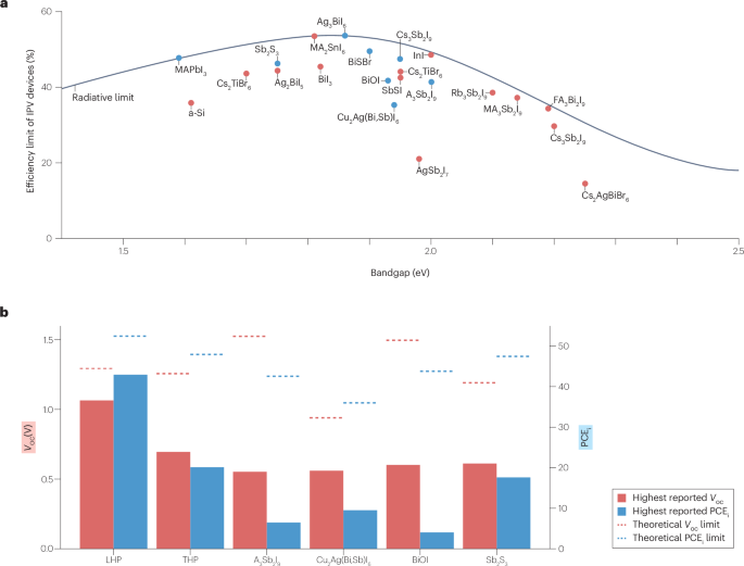
a, Radiative-limited and spectroscopic-limited maximum efficiency (SLME) of ns2 materials under 1,000-lux illumination. The blue dots represent materials specifically discussed in this Review. Calculations are based on the standard white light-emitting diode spectrum (details in ref. 70). b, Highest-reported open-circuit voltage (VOC) and indoor power conversion efficiency (PCEi) of indoor photovoltaics (IPVs) based on the most-studied ns2 materials. Theoretical limit in VOC and PCEi determined from SLME calculations shown as dashed lines. LHP denotes the lead halide perovskite composition that has led to the highest PCEi, which is Cs0.05FA0.70MA0.25PbI2.25Br0.75 (FA, formamidinium; MA, methylammonium). THP denotes the tin halide perovskite composition that has yielded the most efficient IPVs, which is PEA0.15FA0.85SnI2Br with CsF additives. In both cases, reliable data for optical absorption coefficient were not available, and so the theoretical limits shown are the radiative limits for a 1.71-eV (LHP) and 1.6-eV (THP) bandgap semiconductor. The figure highlights progress and potential of ns2 compound semiconductors for IPVs. a-Si, amorphous silicon. Data from ref. 70.
LHP bandgaps can be increased by mixing Br with I in the halide site or by changing the A-site cation from methylammonium (MA) to Cs (that is, CsPbI3)27,36,37. Increasing the bandgap can decrease the stability of the perovskite: mixed iodide–bromide perovskites with high Br content suffer from facile phase separation due to ion migration38, whereas the desired black α-CsPbI3 is not stable compared with the yellow phase36, but these challenges have been addressed by reducing the defect density through use of passivating additives27. LHP IPVs have been tested at illuminances as low as 50 lux, with a report of 8.6% PCEi and 0.67 VOC achieved using an n–i–p architecture by excluding the dopants from the hole-transport layer that would typically be required for operation under 1-sun (120,000-lux) illumination39.
Devices with high operational stabilities have been produced that maintain 91% of the original PCEi after 540 hours of operation at maximum power point tracking under 1,062-lux illumination in a nitrogen environment36. High-efficiency LHP IPV devices (44.72% PCEi at 1,000 lux) maintained 95% of their initial efficiency after 800 h of stability testing under 1-sun illumination in ambient air27; however, fully encapsulated perovskite photovoltaics used in perovskite–silicon tandems have been reported to retain 99.6% of their original efficiency after 8 months of outdoor stability testing40. The more benign conditions found indoors compared with outdoors suggest that further stability enhancements for LHP devices can be achieved.
The VOC of LHP IPV at 1,000-lux illuminance is at 81.5% and the PCEi at 83% of their respective theoretical limits27 (Fig. 3b). This demonstrates that LHPs have rapidly been highly optimized but still have room for improvement. Improved stability and performance will require more effective additives and growth methods to reduce bulk trap densities to increase PCEi, reduce phase separation and increase interface passivation, particularly for the wider-bandgap perovskites that have higher efficiency limits but are more susceptible to non-radiative losses41,42. It will also be important to adopt the encapsulation methods successfully implemented for outdoor photovoltaics43,44.
LHP IPV devices have primarily been demonstrated on the laboratory scale, with device active areas under 1 cm2. Efforts to increase their active area for commercial-scale manufacturing have explored printing on flexible substrates, which would enable continuous manufacturing techniques. Flexible LHP devices deliver lower PCEi values than those based on glass substrates because restrictions on processing temperature, and the surface and wetting properties of the transparent conductive substrate, limit the quality of the transport and interfacial layers, resulting in higher recombination currents45,46. Nevertheless, flexible perovskite IPVs with 30–40% PCEi have been fabricated on low-cost polymer films by increasing the bandgap through compositional engineering47, improving the interfaces of the multilayer stack, application of processes and additives that improve crystallization, passivation of grain boundaries46,48 and releasing mechanical stresses49,50,51. Flexible LHP devices require specific encapsulation solutions, such as a combination of thin-film deposition, multilayer barrier lamination, and thermoplastic or resin adhesives45.
Organic photovoltaics and dye-sensitized solar cells
A strength of OPVs lies in the abundance of carbon-based molecules52. By employing the organic molecule 2-(9H-carbazol-9-yl)-phosphonic acid (2PACz) as the self-assembled hole-transporting layer, as well as in the photoactive blend with PM6:Y6 (device structure: 2-PACz-treated ITO/PM6:Y6:2PACz/electron-transporting layer/Ag), a PCEi of 37% was achieved at 1,000 lux (ref. 53). The relatively low VOC (0.72 V) was due to the low bandgap of 1.4 eV in the blend, so tuning the bandgap for applications under artificial lighting could lead to future improvements. An all-polymer IPV cell with a promising a VOC of 1.16 V has been demonstrated54. Most materials engineering research in OPVs focuses on enhancing the bandgap and the morphological and interfacial structure of the organic mixture to find the optimal balance between JSC, VOC and FF22,55.
The efficiencies of IPVs based on DSSCs have improved, reaching 36–38% by suppressing charge recombination using copper electrolytes with co-sensitization dye and customized ligand additives8,56. The known issue regarding DSSCs is their extensive use of liquid or quasi-liquid ionic mediators. One of the key aspects for manufacturing long-lasting DSSCs modules is to devise robust encapsulation methods to contain the electrolyte between the bottom and top contacts57.
There are other promising IPV technologies, such as kesterites, which offer high stability, direct and tunable bandgaps (1.0–2.0 eV), and flexible processing. They have demonstrated initial PCEi of 6.0–8.6% under white light-emitting diode (WLED) illuminance of approximately 5,000–62,000 lux (ref. 58). Amorphous selenium and quantum dots are noteworthy for their high absorption coefficients and wide bandgaps, which enable efficient indoor light harvesting59,60. Amorphous selenium also promises stable IPV device performance59.
As commercial vendors favour the highest performance possible, all new photovoltaic (PV) technologies are trying to close the efficiency gap with LHP IPV devices. However, consumer electronics markets globally have restrictions on the use of lead61, and this could be a barrier to widespread adoption of LHP for powering IoT electronics. OPV and DSSC technologies have further issues with toxic solvents for industrial fabrication, and a reliance on low-abundance materials for electrolytes and electrodes. As a result, there is a clear need to develop new classes of light-harvesting materials that could address these current sustainability challenges.
Low-toxicity ns
2 compound semiconductors
LHPs can overcome the performance limitations of established IPV materials and have the potential to be manufacturable cost-effectively at scale, with sufficient stability for IoT applications. Unravelling the reasons behind the efficient performance of LHPs will enable researchers to replicate these properties in lead-free compounds that can be made without use of toxic precursors, overcoming the two main limitations of LHPs62. A substantial class of target materials are compounds based on partially oxidized cations with a pair of valence s2 electrons (ns2 compounds). These include tin-based perovskites, chalcogenides and chalcohalides, as well as other Bi-based and Sb-based compounds63. Some of these materials have high theoretical optical limits in performance (that is, SLME; Fig. 2a,) justifying an in-depth evaluation of their potential.
Tin halide perovskites
Tin halide perovskites (THPs) are direct chemical and structural analogues to LHPs, substituting Pb with Sn. Out of all ns2 compounds, THPs have demonstrated the strongest performance63 in solar cells64. Applying these materials for IPVs requires partially substituting iodide with bromide to increase the bandgap from ~1.4 eV (with I:Br = 1:0) to ~1.6 eV (with I:Br = 2:1)65,66. THPs are appealing because they demonstrate lower ecotoxicity than Pb from LHPs62, yet show the favourable optoelectronic properties found in LHPs, including a low Urbach energy, low exciton binding energy, and band-like transport of charge carriers with high mobility67.
Two key limitations of these materials are the facile oxidation of Sn2+ to Sn4+, with ready high p-type doping, and rapid film crystallization that is difficult to control. To address these challenges, FA0.75MA0.25SnI2Br has been doped with Catechin (a phenolic antioxidant), which successfully suppressed Sn4+ formation and improved both the device performance (from 10.45% to 12.81% under 1,000 lux) and stability in air without encapsulation68. Other methods attempted include the introduction of additives (including KSCN, nicotinamide and CsF) to the interface between the tin perovskite and the poly(3,4-ethylenedioxythiophene) polystyrene sulfonate (PEDOT:PSS) hole-transport layer to assist in perovskite crystallization and reduce interface recombination65,67,69.
The most efficient THP IPVs reported so far (20.12%, Table 1) were achieved by introducing CsF additives67. The role of CsF is not clear, but it is believed to influence perovskite crystallization and reduce bulk defect density66. Despite these rapid increases in performance, these devices are still far from their theoretical limits (Fig. 3b), allowing for potential improvements.
Chalcogenides and chalcohalides
BiOI was one of the early ns2 materials considered for IPV70. BiOI has the advantage of forming delocalized free carriers rather than self-trapped carriers71, has a stable bandgap of 1.9 eV and can be made by a scalable chemical vapour deposition method at comparatively low deposition temperatures of around 350 °C (ref. 72). In an early demonstration of these ns2 materials for IPV, a PCEi of 4.0–4.9% under 1,000-lux WLED lighting was reported, with a VOC of 0.60 V (ref. 70), well below the theoretical limits calculated from SLME (Fig. 3b).
The underperformance of BiOI could be due to coupling between charge carriers and longitudinal optical phonons coherently generated following photoexcitation, leading to increased Urbach energies (close to 70 meV in thin films)72,73,74 and an unavoidable non-radiative decay mechanism, which both lower the VOC and limit charge-carrier diffusion lengths, even if the material were defect free71. These factors could inherently prevent BiOI from approaching their SLMEs. Another potential chalcohalide is BiSBr, which has higher SLMEs, over 40% under 1,000-lux WLED lighting75. Although these materials have photoluminescence lifetimes of more than 1 ns at room temperature, they have yet not been demonstrated in IPVs because of challenges in achieving compact morphology as thin films75.
Sb2S3 and Sb2Se3 are some of the most widely explored chalcogenide ns2 compounds, with outdoor PCEi values now reaching 10.75%76. Although Sb2Se3 has a bandgap that is too small for optimal WLED energy harvesting, Sb2S3 has a bandgap of 1.75 eV, which is better suited for this application77 (Fig. 3a). A Sb2S3 IPV device was 16.37% efficient under 1,000-lux WLED illumination78, which improved to 17.55% on reducing the grain boundary density through use of monoethanolamine additives to modulate grain nucleation and growth20,78.
Sb2S3 devices are still performing far under their theoretical peak performance (Fig. 3b), which could be due to self-trapping or defects9,79. A 0.6-eV Stokes shift in photoluminescence compared with the bandgap has been argued to be caused by self-trapping79, but others believe that these observations are trap states formed within the bandgap and that excitations in Sb2S3 form large polarons instead9. Computational studies of Sb2S3 identified the dominant defects to be S and Sb vacancies, which introduce deep levels and are consistent with the deep traps found experimentally80. These are similar to the findings for Sb2Se3, where it was found that such defects could be passivated through oxygen exposure by forming OSe antisites81. It is possible that oxygen passivation could also be effective for Sb2S3.
Other notable ns
2 compounds
Prominent halide materials that have gained interest for IPV are vacancy-ordered triple perovskites and Ag–Bi–I compounds. Vacancy-ordered triple perovskites include Cs3Bi2X9 and Cs3Sb2X9 (where X = Cl, Br or I)82,83,84, and have one in three metal cation sites vacant. Although it is common to find 0D structured materials within this family of compounds (comprising isolated face-sharing octahedra), the dimensionality could be modified to 2D by using smaller species in each of the three sites (such as Rb+ or Cs+ instead of CH3NH3+; Sb3+ instead of Bi3+; Br– instead of I–). Forming a 2D structure improves band dispersion and reduces exciton binding energies83. Thus, efforts with IPV have focused on 2D Cs3Sb2ClxI9−x, which has a bandgap in the range of 1.9–2.0 eV, and reached 4.4% PCEi (ref. 70). Improvements in performance to 6.37% were achieved by using a combination of Cs, MA and formamidinium (FA) in the A-site, which reduced the trap density85.
Ag–Bi–I compounds are a family of materials with tunable stoichiometry and crystal structure, ranging from defect-spinel-structured AgBi2I7, CdCl2-structured AgBiI4 or NaVO2-structured Ag2BiI5 and Ag3BiI6 (refs. 86,87). Owing to the high absorption coefficient, Ag3BiI6 is predicted to have a high SLME of >50% under the standard 1,000-lux WLED spectrum (Fig. 3a). However, the realization of these materials in IPV has been challenging, with PCEi <6% reported for AgBiI4 (ref. 88). The reason for the low performance of Ag–Bi–I IPV remains an open question, and a 2024 paper suggests that this could be due to limited charge-carrier transport, caused by carrier localization in these materials89.
Quaternary Cu–Ag–Bi–I compounds, such as Cu2AgBiI6, show improved mobilities and lower exciton binding energies than AgBiI4, which is advantageous for improving charge-carrier transport lengths90,91. By optimizing the morphology of the films (by adding HI to the precursor solution), as well as alloying Sb into the pnictogen site, the IPV performance was improved from 1.3 ± 0.5% (Cu2AgBiI6 with no HI) to 9.53% under 1,000 lux (Cu2Ag(Sb,Bi)I6)92,93,94.
Performance in real-world settings
High-performance DSSCs and OPVs have promising operational stability22,95, and commercial devices show promise for stable indoor operation96,97. LHP IPVs have demonstrated high operational stability, implying their suitability for practical applications27,36. In emerging ns2 compounds, efforts with mixed iodide–bromide perovskites for IPV have demonstrated that THP devices can be operated in ambient air. For example, FA0.75MA0.25SnI2Br THP IPV retained 80% of the original PCEi after 50 days of storage in a glovebox in the dark (but tested in air at regular intervals)68. Although promising, the stability of THP IPVs has not reached the level of their lead-based counterparts.
Unencapsulated BiOI and Cs3Sb2(I,Cl)9 IPV devices stored for 5 months in an N2-filled glovebox with >1,000 ppm O2 and >500 ppm H2O were found to double in performance. (Cs,MA,FA)3Sb2(I,Cl)9 and Cu2Ag(Bi,Sb)I6 IPVs were found to retain 86% and 82% of the initial PCEi after 28 and 100 days of storage in ambient air without encapsulation85,92. Sb2S3 IPV retained >96% of the initial PCEi after a month of storage in dry air (<15% relative humidity)20. These Bi-based and Sb-based materials have potential as absorber materials in IPV devices that are stable without complex passivation layers.
Practical demonstrations of emerging IPV materials powering IoT include a DSSC IPV cell array (22.4 cm2 total active area) capable of producing a maximum power of 1.87 mW and voltage of 4.62 V, which was used to power IoT sensor prototypes to forecast energy availability in diverse settings such as homes, factories and offices8. Similarly, OPV and LHP IPV minimodules have been used to power many low-power IoT devices, including temperature and humidity meters and RFID integrated circuits98,99. In 2021, small-area (7.25-mm2) BiOI and Cs3Sb2(I,Cl)9 IPV devices produced sufficient photocurrent under indoor lighting (4–6 μA) to power carbon nanotube inverters, which required only 0.6 μA to operate18. In 2024, 5-cm2 Sb2S3 IPV minimodules powered a multisensor platform that communicates by Bluetooth low energy, and these were stable for >14 h under continuous operation, both at 1,000 lux and in a common office area at 726 lux (ref. 20).
Measurements, characterization and standards
Meaningful comparisons of the indoor light conversion performance between different technologies in the literature has been difficult because of the lack of standardized testing conditions for IPV materials. The success of solar PV electricity generation and the global market of solar PV products — from materials to systems — has relied on the wide adoption of a set of standards, which harmonized the testing of devices from a strong global network of measurement facilities and research laboratories100. Standards for solar PV cover all available technologies currently in the market and span power and energy rating, labelling, qualification, reliability and safety standards. These standards ensure confidence in solar PV products and have enabled market growth. By contrast, the necessary standards for the nascent IPV market are underdeveloped.
Device performance testing standards
Early steps towards IPV standard testing were made in 2023 with the publication of the International Electrotechnical Commission (IEC) Technical Specification 62607-7-2:2023 (ref. 101), where the indoor standard testing conditions (ISTCs) for IPV devices are defined, along with requirements for light-source classification and use of calibrated reference devices. In practice, the above technical specification derives from the IEC 60904-X series for solar PV, where current–voltage (I–V) testing and other methods are defined, and many of them can be adapted directly for IPV testing. The major differences between solar and indoor-condition PV testing are the light intensity and spectrum. ISTCs and two reference spectra (along with AM1.5 solar spectrum for comparison) are presented in Fig. 4a and Supplementary Table 1. Note that IEC also accepts any user-defined light source as an alternative to the two examples provided.
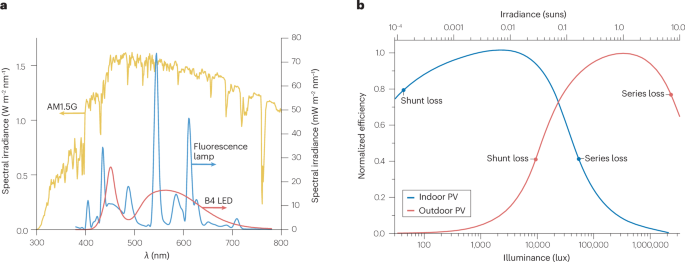
a, The reference spectra for indoor testing, CIE B4 LED and CIE FL10 (fluorescence lamp), with global horizontal irradiance spectrum AM1.5G for comparison. The indoor reference spectra are defined only in the visible region of the spectrum, between 380 nm and 780 nm. b, Single diode model examples of indoor and outdoor photovoltaic (PV) devices, with respective shunt and series resistance losses. Efficiency varies with irradiance, so outdoor photovoltaic devices are optimized for low series resistance, whereas indoor devices are optimized for high shunt resistance.
The indoor reference spectra are defined only in the visible region of the spectrum, between 380 nm and 780 nm. At common indoor low-light conditions, nonlinear power response to irradiance is expected for PV devices. Hence, ISTCs require measurements at three different light levels to ensure that such nonlinearities are captured, and the spectral profile of the light source must be maintained during the measurements at the different light levels102. The ISTC also implies that spectral response measurements for IPV devices need to be acquired at such low light levels and not at 1 sun, otherwise differences might be observed103. Spectral response measurements are useful for PV device development and optimization, and necessary for spectral mismatch calculations that correct differences between light sources. The standard temperature of 25 °C means that PV devices potentially need to be heated slightly, but the low illumination levels mean that temperature control is straightforward to maintain during measurements.
Challenges and gaps in standards
Many testing standards and measurement methods for solar PV can be adopted for IPV characterization, but there are areas where new methods and technical specifications are needed. The accuracy of target IPV device testing relies on the accuracy of primary reference cell calibration, where for solar applications very low uncertainties have been achieved104. Although a few national labs can offer calibrated reference cells for IPV testing as a custom service, commercial off-the-shelf reference cell products and primary reference cell calibration services for IPV device testing will be needed for widespread use in academia, industry and test labs. These devices are a necessary component for IPV testing that will also help the development, commercialization and use of indoor light simulators, with some prototype systems compliant to IEC TS 62607-7-2:2023 already reported105.
New reference cells will need to be combined with international measurement intercomparison activities across different labs around the world to evaluate IEC technical specifications for IPV testing, ensure reproducible results, demonstrate proficiency and establish confidence in new standards. Such intercomparison activities, along with additional studies and data collection regarding the indoor light resource, will also provide evidence on the suitability of the choice of spectrum of IEC TS 62607-7-2:2023 and the overall clarity of the TS. Finally, established efficiency certification services that comply to developed standards will allow a best research-cell efficiency table specifically for indoor light conditions to be established, as has been done for outdoor PV. This comparison will result in a fair gauge for quantifying how IPV technologies develop.
The IEC standard for reliability testing for solar PV products (IEC 61215) has established confidence and improved reliability of solar PV products for outdoor use106. Specific qualification testing technical specifications will be required for IPV devices that reflect the stress levels of indoor environments. The same argument applies for safety standards (such as IEC 61730 safety qualification standards for PV modules) and stress tests. For research and development purposes of new materials and devices in the solar PV area, the International Summit on Organic Photovoltaic Stability (ISOS) protocols are appropriate tools for relevant stress tests of OPV devices107 and have also been expanded to LHP materials and devices108.
Adding protocols relevant to IPV conditions and adoption by the IPV community will allow data comparison and the identification of relevant degradation factors and failure mechanisms under indoor light conditions. With the wider adoption and market penetration of IPV devices, standards and best practices will keep improving and developing, as has been the case for solar PV, where standards are still being created and revised as technology progresses.
Characterization of optimal IPV performance
The low-light performance of IPV devices can be affected by spectral response, series and shunt resistances, and linearity effects. These phenomena depend on both the material and the PV device architecture, such as the number of cells and the cell size. For indoor applications, having a higher series resistance than in outdoor PV applications can be tolerated because the lower currents (of the order of microamps) lead to lower voltage and power losses. Achieving high shunt resistance is much more important for high-efficiency IPV devices (Fig. 4b). These difference in desired shunt and series resistance for IPV device design architecture allow for modules with different structures7. Characterization techniques that detect shunts, or determine the spatial profile of shunt resistance, are important for the development and quality control of IPV devices.
Nonlinearity effects of photocurrent and photovoltage of IPV devices as a function of irradiance are important under indoor light conditions, hence the requirements for testing at different illuminance levels. Although for outdoor applications nonlinearity of photocurrent is important in order to evaluate low-light-condition losses, for IPV in IoT applications the behaviour of photovoltage as a function of illuminance levels is much more important. This is because IPV devices are likely to be used to charge batteries, and this requires a minimum voltage level to be delivered.
Resource and device modelling
The indoor light resource is challenging to predict across different sectors and settings, and will depend on specific cases and applications. Initial efforts have been made to assess the availability of indoor light resources for energy harvesting15 or develop models for indoor light-harvesting systems109, but more validated modelling tools for indoor light harvesting are needed. Stronger modelling is necessary for IoT system integrators, and for increased market penetration of indoor light-harvesting products8. Improved assessment of the indoor light resource with regards to availability, spectrum, intensity and variability will also feed into PV device modelling and simulation requirements for IPV technology material and device optimization.
Datasets of indoor light resources will also inform future revisions of IEC TS 62607-7-2:2023 regarding choice of spectrum and intensity levels. Such data will also allow the development of energy rating standards for IPV products, similar to the IEC 61853 series for solar PV, which also include reference climate-specific datasets. In addition, the potential extreme limits under indoor light-harvesting conditions (maximum irradiance, temperature and humidity) will define relevant safety and reliability standards that will ensure the quality of IPV products, thereby increasing confidence in these devices.
Scalability and integration
IPV scale-up and integration from lab prototypes to commercial products involve only marginally increasing the device size from small (1 cm2 or below) to large (>1 m2) area. The area required depends on the specific application, with some applications, such as smart dust, requiring small-area devices with a low footprint7,110. The adoption of flexible substrates can aid the integration of the IPV in a specific product, owing to their capacity for installation on curved or bendable surfaces. Furthermore, flexible substrates offer a broader range of application scenarios, thanks to their lightweight and adaptable nature: from indoor building-integrated photovoltaics to wearables (digital watches, smart textiles and human-borne sensors) and consumer appliances (wireless sensors, digital gadgets and small displays)111.
Scalability
Techniques compatible with industrial production, and based either on solution or on physical deposition techniques or on a combination of both112, have been demonstrated for OPV, DSSC and LHP technologies. The aim of the PV sector has been to increase the module area while maintaining high efficiency, as the focus so far has been maximizing energy output in outdoor operation113,114,115.
Large-area devices have been realized across DSSC, OPV and LHP technologies and have been tested at 1,000-lux illumination (Fig. 5). A rigid-module DSSC with an area of 26.80 cm2 and PCEi of 11.25% has been reported. The same paper also reported flexible modules with the same area and efficiencies of 10%116. Rigid OPV devices with 1.5-cm2 area have a record PCEi of above 30%10, while on flexible substrates with 13.6-cm2 area, an all-printed eight-cell module fabricated via roll-to-roll processing had a PCEi of 13%117. LHP IPVs on rigid substrate that used a wide-bandgap perovskite with an area of 12.96 cm2 had a PCEi of 43.5%11, while on flexible substrates, a device with 12.96-cm2 area achieved a remarkable 31.7% PCEi (ref. 118).
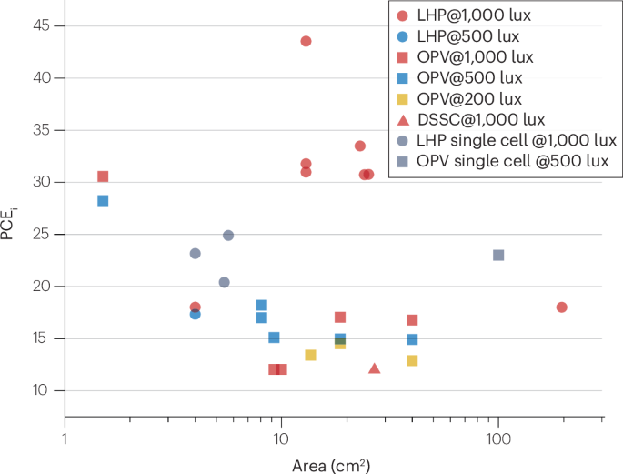
Reported performance of selected large-area lead halide perovskite (LHP), organic photovoltaic (OPV) and dye-sensitized solar cell (DSSC) at different illumination intensities (data available in Supplementary Table 3). PCEi, indoor power conversion efficiency.
Most reported devices are produced using spin coating, a reliable process for fabricating solar cells and modules at the laboratory scale, with few reports thus far on fabrication techniques compatible with large-area production. An all-printed carbon perovskite solar module — in which the different layers were spray coated, screen printed or infiltrated — is one of the few examples of all-printed large-area (196 cm2) indoor perovskite modules with a PCEi of 16% at 1,000 lux (ref. 119), but with the major drawback that the high-temperature processing conditions cannot be applied to flexible substrates, preventing continuous manufacture. A 23-cm2-area module reached a PCEi of 33.49% at 1,000 lux with a p–i–n device configuration. Both electron-transport and hole-transport layers were deposited using large-area printing techniques (low-angle blade coating and shear coating, respectively), whereas the perovskite had to be spin coated120. This confirms that the most challenging aspect of LHP IPV scalability is the deposition of the LHP layer, whose quality is strongly affected by the environment and the deposition method used.
For OPV, large-area modules have been demonstrated using different printing techniques, such as blade10,121 and slot-die coating122, and roll-to-roll fully printed modules on flexible substrates117. The adoption of flexible substrates can aid the integration of the IPV in an IoT node and enable roll-to-roll manufacturing, leading to low-cost and high-throughput serial production of IPV cells and modules. The challenge in the fabrication process is the need to find non-halogenated organic solvents for processing, as these are too toxic for commercially available products122.
Unlike PV for outdoor applications, IPV operation is not critically affected by sheet resistances — and thus the cell size. Individual OPV cells with areas as large as 100 cm2 can easily deliver 23% PCEi under LED illumination of 500 lux, only slightly lower than cells with an area two orders of magnitude smaller (1 cm2) that deliver 26% PCEi (ref. 123). Many IoT applications require voltages >1 V, such as energy-storage supercapacitors, which cannot be reached with an individual cell. Modules, in which cells are connected in series, are the more likely candidates for seamless integration of the IPV in a IoT device or platform. The process to obtain the series interconnections must be optimized, reducing as much as possible the shunt resistances that affects the performance of IPV devices, especially at low light intensities. In particular, laser patterning must be carefully carried out to avoid leaving conductive debris on the interconnection area, which could lead to shunt paths. Guidelines have been proposed for designing IPV modules to reduce the effects of shunts and increase the overall efficiency of the module110.
Integration
Indoor lighting has substantially lower power density than outdoor light. A commercially available OPV module operating in a semiconductor manufacturing clean room would produce around 300 J (83 mWh) of energy in a typical 24-hour period15. To put this in perspective, a similar amount of energy can be released by burning 10.9 mg (fuel required for 300 J) of methane (50 J mg−1 specific energy) at 55% thermal efficiency (27.5 J mg−1). Given these low power outputs, it is crucial that the whole IPV–IoT system be as efficient as possible. IPV modules must be very efficient in ambient lighting and also must be able to maintain a specified maximum power voltage for efficient power conversion by the energy-harvesting electronics even at the lowest light levels. Additionally, the choice of both electronic components and storage elements must be carefully considered to avoid losses wherever possible.
In terms of IPV module design for a given PV technology, multiple series-connected cells might be preferred for maintaining a specific voltage even at low light intensities to keep the system in its most efficient state. An alternative strategy would be to use power management specifically designed to operate at lower voltages more commonly seen in single PV cells. It is important, therefore, to choose the most appropriate power management hardware for the chosen PV technology and operating conditions, to extract the maximum amount of energy.
Another important consideration is the stability of the IPV modules under ambient conditions. An IoT node, such as a sensor, could be in operation typically 1–5 years, and the lifetime of the IPV module must exceed that of the IoT node. It is both possible and desirable from a sustainability point of view that IPVs might extend this lifetime owing to batteries not needing replacing or recharging. Fortunately for IPVs, the environment indoors is far less demanding than outdoors owing to minimal ultraviolet radiation, lower light intensities, and stable humidity and temperature. Extrapolated stabilities of 30,000 hours (ref. 124) and 34,000 hours (ref. 125) have been demonstrated for OPVs. Perovskites have exhibited stabilities of >1,0000 hours under 1 sun (ref. 126), and so it is likely that indoor stability will far exceed this.
Sustainability and commercialization
IPV development has mostly prioritized performance and cost targets, without sufficient attention to the environmental impact of the materials used and how the devices are processed127,128. The sustainability focus has been limited to the absorber layer, without considering the device’s entire life cycle. It will be essential to consider the acquisition and synthesis of raw materials, device fabrication, disassembly, and material recovery at the end of life (EOL) to ensure the overall sustainability of a device129. Commercialization of emerging PV technologies presents several technoeconomic challenges, such as scaling up production from individual cells to modules without compromising on performance, achieving stability in line with the products they power, and cost-effectiveness.
Sustainability challenges
To study the entire life cycle of a device, eco-design should be established as a core and essential element in the sustainable development of IPVs. In this context, life cycle assessment (LCA), which designs a product by accounting for the environmental impact of the materials and processes used, can provide valuable insights to address the challenges associated with emerging products. LCA can help to model reliable, innovative technological value chains that are scalable and reproducible, and, importantly, adhere to the principles of the circular economy130. Furthermore, the flexibility of the LCA methodological framework would help in including other discriminating aspects, such as hazardous and critical materials, in alignment with international regulations28,131,132 and voluntary approaches to guide the innovation process for chemicals and materials133.
LCA studies in the scientific literature on IPVs are limited by the very early stage of research and development, as well as by the fragmentation of this sector3, and by the absence of a harmonized LCA modelling standard to guide prospective investigation and enhance the comparability among results from different groups or companies134. Given the large potential size of the IoT market1,3,135, the availability of robust LCA data is essential for innovation and providing solid scientific evidence for decision-making. Examples from the outdoor utility-scale PV sector can guide systemic analyses of various aspects of the value chains: the resource demand for IPV technologies, relative global supply availability and identification of plausible alternatives for critical and strategic materials136, health and ecotoxicity of chemicals and solvents for producing IPV devices137, and the EOL strategies to ensure the most rational and effective design-for-recycling of IPV products138,139.
Developing low-toxicity solvents is critical for precursor synthesis in the manufacture of IPV devices140, and it is essential to consider the complexity of the production processes and the current technological readiness of industrial production136. It is also important to consider the sustainability of the electrodes and substrates that represent a large fraction of the overall weight of the device and tend to dominate the environmental profile, with contributions exceeding 90% in almost all LCA impact categories, as reported in the literature for outdoor PV141,142. It is especially important to substitute critical elements (such as Au, Ag, In) with more widely abundant materials, such as Al or carbon-based alternatives, without compromising on efficiency and/or stability.
Pb and Cd are regulated in the electronics market, so designing active materials that include them, such as LHPs, PbS quantum dots, and the CdS commonly used as buffer layers in chalcogenide devices, requires careful consideration. Substituting Sn or other elements for Pb in LHPs leads to a substantial reduction in performance and/or stability143,144. Efforts are underway to prevent Pb release through sequestration, using materials that bind to Pb2+ such as supramolecular complexes. These materials, either fixed to the device or integrated into the semiconductor143,144,145,146,147, have shown short-term effectiveness, but long-term effectiveness over the >10-year lifetime of an IPV needs investigation.
Singfilm Solar calculated their Pb content to be 30 ppm, while Saule Technologies report a Pb content close to the order of 1 ppm. Singfilm have stated that their calculation accounted for the mass of the substrate and encapsulants, as the LHP is a thin film. But other work has shown that not considering the encapsulants to be part of the homogeneous layer, and using a thin flexible substrate, can lead to the Pb content exceeding the 1,000-ppm threshold61.
The development of advanced encapsulants for LHP PV for outdoor installations opens up the possibility of implementing new approaches where the encapsulation not only provides robust long-term protection during operation but is also optimized for EOL recycling. Among state-of-the-art IPV technologies, there are already examples of recycling for some of the critical materials and a few components. However, these aspects are still either in their early infancy on the laboratory scale (such as for OPV and DSSC, LHP) or not considered at all for some technologies (such as Pb-free ns2 absorbers for IPV) because the research is too immature148,149.
Commercialization challenges
a-Si:H, OPV, DSSCs and III–V materials have all entered commercial production and have benefited from many decades of effort to develop consistent, reliable performance in large-area modules. a-Si:H is made by plasma-enhanced chemical vapour deposition, and there is now little difference in the performance of lab-scale versus commercial-scale cells150,151. III–V materials are also fabricated by vapour deposition152, but OPVs and DSSCs can be manufactured by solution processing. Several companies are manufacturing OPV by roll-to-roll processing, with over a million square metres of annual capacity153,154,155. For DSSCs, modules have been manufactured since 2009 on both rigid and flexible substrates97,156, and the current market is worth more than US$100 million157.
Moving from liquid-based DSSCs to the more stable and robust solid-state devices will require further advances8, as will the development of more sustainable light sensitizers35 that are better matched with indoor light spectra35. A key aspect for long-lasting DSSC modules is robust encapsulation methods to contain the electrolyte between the bottom and top contact. Smaller devices required for powering the IoT face fewer encapsulation issues than their outdoor counterparts21,158. However, for flexible devices, maintaining a liquid between two mechanically non-robust films — the substrate and the permeation barrier159 — remains a challenge that requires not only solid or quasi-solid-state mediators, but also creative containment solutions.
If IPVs are to be used to power the IoT, the device area would need to be tens of square centimetres to produce sufficient power7, and millions of these IPVs would need to be produced per year, such that the production output should be at least several thousand square metres per year. This output is still orders of magnitude lower than the requirement for outdoor PVs160, and producing several thousand square metres per year of PVs is within the capabilities of a megawatt-level thin-film PV manufacturing facility161,162.
Emerging halide inorganic semiconductors — currently deposited by spin coating — can benefit from the developments in LHPs, as similar solvents are used to prepare these materials. For example, BiOI is made by chemical vapour deposition72, and Sb2S3 can be made by vapour transport deposition163,164 or close-space sublimation165,166. These production techniques are similar to the methods used commercially to grow CdTe thin-film solar cells from vapour deposition, and the challenge will be to control the morphology and uniformity of the films when prepared over areas larger than 10 cm2 (refs. 167,168).
Technoeconomic barriers
Technologies with low capital intensity could face lower barriers to commercialization3, and they are primed to offer advantages with their simple manufacturing processes and equipment that even allow customization of device layouts for end-users in short time frames. At high volume levels — tens of millions of identical PV devices — the capital expenditure weight on the cost will decrease, and materials and throughput will become fundamental3. The technical and financial costs of shipping and integration in a third-party electronic product become more important, and direct licensing or joint development agreements with the manufacturer of the end product could be viable solutions169.
Producers, integrators and end-users need to account for the policy landscape when adopting new technologies for IPV. The European Union has driven circular economy initiatives applicable to LHP technology through directives such as Waste Electrical and Electronic Equipment (WEEE)170. WEEE, the fastest-growing waste stream globally at 53.6 Mt per year, represents a large challenge. WEEE directives promote circular economy principles by banning WEEE landfilling, setting recycling targets and enforcing extended producer responsibility, which makes producers responsible for the EOL costs of the products. Similar laws exist in China, Japan and California171.
Indoor environments are milder, and product lifetimes are within 5–10 years, making IPV an easier market to enter than the outdoor PV market (product lifetimes >25 years under harsh stressors including infrared and ultraviolet irradiation). However, PV devices operating indoors are more sensitive to the creation of defects during ageing, leading to faster degradation of performance compared with the same device measured at standard test conditions172.
Flexible devices seem the more suited for seamless integration, but plastic films are known to lead to faster ingress of water vapour compared with glass43,173,174. More investigations should be carried out into this differential ageing, stable material architectures and effective encapsulation methods. Most research has focused on small laboratory cells, but upscaling the technology can increase the density of defects. Therefore, it is important to devise deposition, patterning and cell connection schemes that can keep defect densities low, to keep the PCEis of commercial modules close to laboratory values175,176,177,178.
The IoT aims to become ubiquitous, so lowering costs is paramount. The primary economic benefit of IPV — the replacement of batteries at low cost — will not be simple for new PV technologies that have not yet accrued economies of scale. A selected number of companies that can deliver on all aspects of performance, cost and ease of integration will become the leaders in IPV.
Summary and future perspectives
The global market for IoT is expected to grow to over a trillion dollars by 2035 (ref. 3). This growth represents a unique opportunity for unconventional and new PV technologies to power IoT devices in a sustainable and cost-effective way. Despite extensive IPV research and many established technologies showing promising performance across various indoor light intensities, key elements like reliability and sustainability throughout the lifetime of the device are still not fully realized134. As of today, a-Si:H dominates the IPV market, with OPV now growing1. Although it is premature to identify the most promising next-generation IPV technologies, the main features of a promising IPV technology are high efficiency under varying indoor conditions, low manufacturing costs and energy requirements, stability, reliability and non-toxicity. Through this Review, we have identified the five key areas representing important future directions (Box 1).
First, composition engineering is crucial for enhancing the performance of emerging IPV candidates. For DSSCs, new dye molecules with broader absorption spectra, higher molar extinction coefficients and better energy-level alignment can improve PCEi. Solid or quasi-solid electrolytes and containment strategies for flexible devices are essential for stability. For OPVs, developing organic semiconductors with a better spectral match to indoor light sources is a priority. Low-toxicity semiconductors with wide bandgaps, based on inorganic and hybrid organic–inorganic materials, especially those with chalcogenide ions, are promising owing to their high stability. The search for defect-tolerant materials like LHPs could lead to other promising perovskite-inspired IPV absorbers.
Second, high device operational stability is crucial to ensure commercial compatibility with the multiyear lifespan of IoT devices. The devices should perform under a wide range of indoor light conditions. Fabrication of high-quality absorber layers will ensure reduced leakage current and bulk recombination losses. The use of advanced AI algorithms can accelerate and enrich tailored device optimization and data interpretation, thus boosting the development of efficient IPV technologies. It is also important to place more emphasis on developing effective encapsulation that is suitable for the specific application (such as on rigid substrates, or for wearable applications).
Third, harmonized performance assessment methods are crucial, such as the recent IEC TS 62607-7-2:2023, where ISTCs and procedures are defined. Additional harmonization efforts will be needed, specifically for appropriate stress tests, qualification standards and energy rating assessment under indoor conditions. The harmonization efforts will require investigations of the indoor light resource, which will also allow for the development of yield modelling tools. Methods that reveal shunt resistance values and its uniformity, as well as power linearity under low-light conditions, will be critical for IPV technology development.
Finally, energy management and storage are crucial for efficiently powering IoT devices. Efficient power converters and innovative energy-storage systems such as supercapacitors179,180 can ensure a steady power supply to indoor devices, even in low light. Collaboration between PV experts and IoT engineers is essential. The development of IPV technologies must consider sustainability across the value chain, including raw materials, scalable production methods and recycling strategies. Emerging PV companies are focusing on flexible PV and indoor light-harvesting markets. Customizable shapes, even on flexible films, make emerging IPV technologies appealing and versatile for diverse IoT needs.

Responses