Quantum materials for spintronic applications

Introduction
Spintronic devices have demonstrated their advantages across various areas. Instead of using the charge degree of freedom of electrons, the spin degree of freedom provides new opportunities in designing high-performance devices. Notably, magnetic sensors based on tunneling magnetoresistance (TMR) exhibit much greater sensitivity than traditional Hall sensors and, therefore, are widely used in ultralow magnetic field sensing such as the read heads of hard-disk drives (HDD). Moreover, the non-volatile nature of spin is promising for the development of next-generation magnetic random-access memory (MRAM). Significant efforts have been devoted to achieving high-intensity, high-speed, and low-power-consumption spin operations. One of the explorations involves combining spintronics with quantum materials1. In quantum materials, quantum effects play an active role in determining the macroscopic physical properties. Magnetism is one of the macroscopic quantum phenomena that have been intensively investigated and utilized, and thus quantum materials are naturally within the scope of spintronics.
The key challenge of spintronics lies in manipulating the interplay between charge and spin. Electrically switching the spin orientation in ferromagnets is required to achieve data recording and computing by spin operation, where spin-to-charge and charge-to-spin processes play essential roles. Spin-orbit torque (SOT) is among the most attractive methods due to its excellent writing efficiency to electrically manipulate magnetic order2,3,4. By utilizing the spin-orbit interaction, the SOT technique generates a spin current, offering advantages over spin-transfer torque (STT), such as lower power consumption5 and faster device operation6. A typical SOT device comprises a bilayer structure consisting of a ferromagnetic (FM) layer and a nonmagnetic (NM) material, with an oxide layer serving as a cap3,7. The traditional discovery of heavy metals (HMs) with larger spin-orbit coupling (SOC) as the SOT source became a milestone in this field, inspiring researchers to seek new materials for improved performance3,8. Enhancing the efficiency of SOT is crucial for reducing the power consumption of spintronic devices. The emergence of quantum materials introduces novel ingredients into spintronics, incorporating strong correlations, breaking symmetry, band topology, collective excitation, and quantum confinement start to contribute, particularly in topological materials9,10,11,12 and strongly correlated oxide materials13,14,15. Combining with a wide variety of two-dimensional materials as the recording layer has opened new prospects for innovative spintronic device16,17,18,19. Furthermore, the intrinsic stability and high resonance frequencies of antiferromagnetic materials distinguish them apart from ferromagnets, within antiferromagnetic spintronics devices showing the broader contexts of spin transport and dynamics20,21,22,23. The recent discovery of altermagnetic materials24,25,26, which exhibits a distinct spin-splitting torque (SST) arising from nonrelativistic anisotropic spin band splitting, independent of SOC, highlights the potential for controllable spin polarization27. The merging of quantum materials and spintronics has also yielded exciting results in the past 5 years, including low energy-cost devices, high TMR ratio, and field-free perpendicular magnetization switching, among others28. It is anticipated that the studies on quantum materials will pave the way for the development of high-performance spintronic devices.
In this paper, we review recent progress in the material requirements for spintronics in various types of materials and summarize the influence of quantum effects in enhancing functionalization. With the widespread presence of spin-orbit coupling, SOTs offer efficient and versatile methods for controlling the magnetic state and dynamics across various classes of materials. One crucial aspect of a spintronic device is the transition of writing layers from traditional transport (HM) to quantum transport (topological materials and strongly correlated oxide materials). Additionally, the recording layers employ two-dimensional magnetic materials, integrating low-dimensional materials into the next-generation spintronic applications. Furthermore, the introduction of antiferromagnetic and altermagnetic materials makes them suitable for high-density memories with minimal inter-bit dipole interactions and fast write times. We also discuss how quantum effects contribute to the functionalization of spintronic devices, which cannot be explained classically. Finally, we discuss the feasibility of integrating these quantum materials in the complementary metal-oxide semiconductor (CMOS) industry and provide a brief conclusion and outlook on how quantum materials facilitate the practical applications of spintronics.
Spintronics device materials
This section provides an overview of the material requirements for spintronics and investigates the role of quantum effects. Spintronic devices primarily comprise writing layers and magnetic recording layers, each playing crucial roles in their functionality and performance. Section II.A presents a brief review of the writing layer of spintronic devices from classical transport to quantum transport with special topological properties corresponding to topological insulators, followed in Section II.B by the review of the strongly correlated oxide materials with rich physical properties and excellent lattice compatibility. Section II.C summarizes the magnetic recording layer of spintronic devices with two-dimensional magnetic materials providing a new platform for spintronic devices achieving the ultimate limit of single-layer magnetic storage and enhancing the magnetoresistance ratio of magnetic tunnel junctions. Next, Section II.D discusses antiferromagnetic material, highlighting its suitability for high-density memories and fast write times. Additionally, it explores the recent discovery of altermagnetic materials, which exhibit a nonrelativistic altermagnetic spin-splitting effect, further enhancing their multifaceted properties and potential applications across diverse fields.
Topological insulators
The primary function of spintronic devices is to achieve spin injection, control, and storage of spin or magnetic states. Currently, research on spintronic devices predominantly focuses on heterojunctions of 5d heavy metals (such as Pt, W, Ta, Hf, etc.) with ferromagnetic metals. However, the efficiency of charge-to-spin conversion based on traditional heavy metal materials remains low, necessitating higher current densities to generate sufficient spin-orbit torque for driving magnetic moment flipping. This increase in power consumption poses a challenge to device performance. Addressing these issues is pivotal for further advancing device development and practical application. New quantum materials, including topological insulators (TIs), offer promising avenues for tackling the challenges due to their unique quantum and structural properties. Consequently, they have emerged as a focal point of research in the field of spintronics.
In recent years, TIs have emerged as prominent materials for spintronics29,30,31,32,33,34,35,36. TIs exhibit insulating bulk states while possessing conductive surface states protected by time-reversal symmetry. The inversion of valence and conduction bands, induced by strong spin-orbit-coupling (SOC) in the material, forms these surface states with a Dirac linear scattering relationship in their band structure. Electrons in the topological surface state exhibit spin-momentum-locking, where the momentum and spin are locked in mutually perpendicular directions37,38,39. Due to the protection of time-reversal symmetry, surface state electrons are immune to the influence of nonmagnetic defects and impurities. These lead to enhanced charge-spin conversion efficiency and reduced critical switching current density when utilizing topological insulators as the SOC layer in spintronics devices.
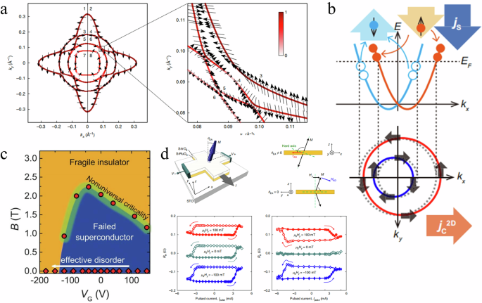
The SOT effect based on topological insulators was initially discovered in heterostructures of in-plane anisotropic magnetic metals, including NiFe and CoFeB, as shown in Fig. 1a,b40,41,42. Subsequently, researchers extended their investigations to ferromagnets and ferrimagnets with bulk perpendicular magnetic anisotropy (PMA), and magnetic multilayers with buffer layers as magnetic layers, observing high SOT in PMA heterostructures. Figure 1c,d show that these structures’ critical switching current density (Jc) was 105 – 106A/cm², representing a significant reduction compared to traditional heavy metal systems3,43,44,45. Notably, the influence of factors such as the spin current shunt effect caused by the high resistance of the topological insulators; the energy band hybridization or magnetic proximity effects at the interface between the topological insulators and the magnetic layer; the quality of the topological insulators (crystallinity, surface defects, carrier concentration); measurement temperature and interface spin transparency, contribute to variations in spin Hall angle (SHA) across different topological insulator/magnetic heterostructures46,47,48,49,50. Additionally, researchers have employed methods such as doping and gate voltage adjustment to control the position of the Fermi level, revealing insights into the relationship between the Fermi level, topological surface state, and charge-spin conversion efficiency29,33,50.

a Schematic diagram of the ST-FMR measurement setup. Adopted from ref. 40. b A typical ST-FMR signal from a Bi2Se3/CoFeB device at 6 GHz. Adopted from ref. 40. c Schematic of the switching sample stack structure, where HSO and τSO are current-induced spin-orbit field and spin-orbit torque, respectively. Adopted from ref. 46. d Current-induced switching of the magnetization due to the SOT that arises from the BixSe(1-x) underlayer in the presence of constant 80 Oe (Jc ~4.3 × 10⁵ A/cm2). Adopted from ref. 46. e Schematic of 3-terminal STT + SOT driven TI-pMTJ device. Adopted from ref. 12. f Field-free SOT switching loop in the TI-pMTJ device under the assisted STT current density JSTT = 1.2 × 10⁴ A/cm2. Adopted from ref. 12.
Currently, spin-orbit torque magnetic random-access memory (SOT-MRAM) stands out as a recognized mainstream solution for the next generation of MRAM technology after STT-MRAM2,3. The device-level integration of topological insulators and magnetic tunnel junctions (TIs-MTJ) is crucial for advancing the industrial application of topological insulator-driven SOT-MRAM technology, as presented in Fig. 1e, f. In recent developments, researchers have combined topological insulators with magnetic tunnel junctions, including in-plane magnetic anisotropy (TIs-iMTJ) and perpendicular magnetic anisotropy (TIs-pMTJ) MTJ devices9,12. Using the third-generation topological insulator (BiSb)2Te3, they successfully fabricated room temperature SOT-MRAM devices, achieving high TMR ratios (~100%) and SOT writing operations (~105 A/cm2) at room temperature. These devices’ critical switching current density is 1–2 orders of magnitude lower than that in current heavy metal-based devices, highlighting the significant potential of topological insulators in the magnetic memory industry12.
Transition metal oxides
The transition to quantum transport in the writing layers, facilitated by the utilization of strongly correlated oxide materials, has also become an important research area due to the emergence of novel quantum effects. Transition metal oxides are widely explored in the field of spintronics due to their rich physical properties and excellent lattice compatibility. They exhibit highly adjustable novel quantum states, such as Mott insulators, topological insulators, topological semimetals, and axion insulators. These states emerge from the intricate interplay between spin, orbitals, charge, and lattice degrees of freedom. Moreover, at the interfaces/surfaces of oxide heterostructures, the disruption of spatial inversion symmetry gives rise to surface states that differ from the electronic structure found in the bulk.
The current emphasis in oxide research revolves around leveraging the SOC properties of transition metal oxides to manipulate their magnetism. SrTiO3 stands out as a representative material, and in 2004, Harold et al. 51 discovered that charge transfer or oxygen vacancies at the surface and heterostructure interfaces of SrTiO3 result in band bending and electronic doping. This confines electrons to a few nanometers perpendicular to the surface/interface, forming a highly conductive two-dimensional electron gas (2DEG), which exhibits remarkable controllable magnetic and electronic transport properties, superconductivity, and quantum Hall effects52,53. Using angle-resolved photoemission spectroscopy (ARPES), Vaz et al. 15 confirmed the existence of these complex bands in the surface electronic structure of SrTiO3, as shown in Fig. 2a, highlighting a significant spin-to-charge conversion efficiency in the 2DEG at the interface. Moreover, they emphasized that at certain band intersections, band inversion and nontrivial topological states may emerge, leading to enhanced spin splitting. Recently, Kaneta-Takada et al. 14 constructed a fully oxide epitaxial heterostructure, SrTiO3/LaTiO3+d. At the interface, a 2DEG is formed, and the exceptionally high conversation efficiency λIEE ~190 nm has been observed through spin-pumping ferromagnetic-resonance voltage measurements (Fig. 2b). To further explore 2DEG systems, the 5d oxide potassium tantalate (KTaO3) has been proposed. It shares similar physical properties with SrTiO3, but KTaO3 possesses stronger SOC, and its electronic structure and charge-spin conversion properties are more sensitive and adjustable. Liu et al. 54 reported two-dimensional superconductivity at the interface of EuO/KTaO3 (111), with a superconducting transition temperature an order of magnitude higher than the SrTiO3 system. Chen et al. 55 demonstrated that this superconductivity can be controlled by an electric field, transitioning continuously from superconductor to insulator with varying gate voltage (Fig. 2c). Zhang et al. 56 further injected a charge flow of 1 nA through the KTaO3/EuO interface 2DEG system using thermal spin injection, showing a charge-spin conversion efficiency significantly higher than the classical Pt/YIG system.
a The calculated spin distribution at the STO Fermi plane. Adopted from ref. 15. b Schematic illustration of the inverse Edelstein effect. Adopted from ref. 14. c VG-B phase diagram of LAO/KTO interface. Adopted from ref. 55. d Current-induced magnetization switching in SrIrO3/SrRuO3 bilayers. Adopted from ref. 58.
Another class of transition metal oxide materials drawing attention in the field of spintronics is the Srn+1RunO3n+1 series. Among them, Sr3Ru2O7 exhibits novel itinerant magnetism, Sr2RuO4 displays unconventional p-wave superconductivity, and SrRuO3 features itinerant ferromagnetism, strong magnetic anisotropy, and high thermal and chemical stability56,57. Chen et al. demonstrated the presence of the topological Hall effect (THE) in SrRuO3 monolayers with thickness ranging from 3 to 6 nm, tunable continuously with an applied electric field13. They attributed THE to the large charge of ruthenium ions and the destruction of inversion symmetry (mainly from the interface) producing the Dzyaloshinskii-Moriya interaction (DMI). Additionally, they designed and prepared SrIrO3/SrRuO3 heterostructures. Owing to the strong SOC in SrIrO3, non-equilibrium spin accumulation can be generated under applied current thus inducing spin-orbit torque (SOT) in the adjacent magnetic SrRuO3 layer. Based on this structure, controlling the polarity of the input current allowed for the directional reversal of magnetization. More importantly, by controlling the oxygen pressure during the growth of SrRuO3 films, the easy axis of magnetization could be continuously adjusted away from the vertical direction. This broke the rotational symmetry of SOT, achieving current-driven magnetization switching without an external magnetic field (Fig. 2d)58.
TMOs have highly complex crystal structures and compositions, and therefore, the synthesis of TMOs with ideal properties requires precise control of the growth conditions, such as elemental stoichiometry, oxygen concentration, strain, and so on, due to the small changes would produce significant differences in phases and properties59,60.
Two-dimensional materials
Two-dimensional (2D) van der Waals magnets are attractive candidates for spin storage due to their novel magnetic and transport properties. They are atomically thin and hold sharp interfaces when building functional heterostructures, thus guaranteeing uniform charge and spin tunneling, potentially achieving single-atom-layer spin storage and enhancing TMR performance. The existence of long-range magnetic order in the 2D isotropic system was initially questioned according to the Mermin-Wagner theorem61. However, magnetic anisotropy is expected to counteract the thermal fluctuation, enabling the emergence of intrinsic ferromagnetism in anisotropic materials such as Cr2Ge2Te662 and CrI363. This has spurred exploration into magnetism in 2D materials64,65,66,67,68,69,70,71. Subsequently, materials with higher Curie temperatures or Néel temperatures, like Fe3GeTe272 and CrSBr73 were discovered. Following this, 2D magnets with ambient temperatures, such as Fe3GaTe274 and CrTe275 were investigated.
The magnetism of 2D magnets can be modulated through varieties of approaches. A practical method of this modulation involves layer stacking and twisting. The interlayer coupling is primarily governed by super-exchange interactions. Different stacking structures of CrBr3 (Fig. 3a) and CrI3 present different magnetism: two stacking models correspond to ferromagnetism (FM) and antiferromagnetism (AFM), respectively76. In Fig. 3b, through twist engineering, different stacking orders could coexist in a moiré structure, and corresponding magnetic orders also coexist, as the result of competition between the interlayer antiferromagnetic coupling and the energy cost for forming FM-AFM domain walls77,78.
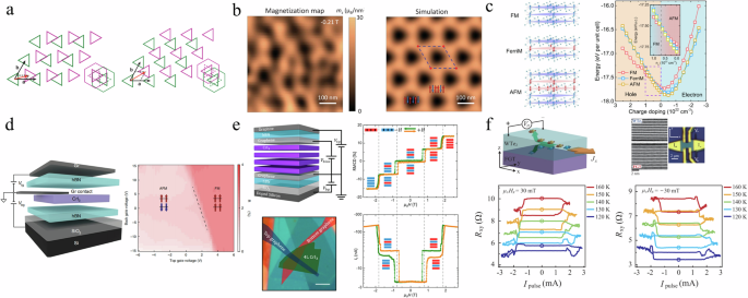
a H-type stacking (right) and R-type stacking (left), corresponding to ferromagnetism and type-A antiferromagnetism, respectively. Adopted from ref. 76. b Magnetization map revealing a signature of periodicity in hexagonal meshes measured at −0.21 T. And simulation of the reconstructed magnetization map based on the predicted magnetic structures (Insets), the corresponding magnetic states. Adopted from ref. 78. c Three potential magnetic configurations for Cr1.2Te2 and total energy as a function of charge density with three magnetic configurations. Adopted from ref. 83. d Gated device structure and RMCD signal of the device when sweeping both the graphite top gate and silicon back gate. The pink region and red region correspond to the AFM state and FM state, respectively. Adopted from ref. 85. e Voltage control of TMR based on CrI3, reflective magnetic circular dichroism (RMCD) signal as a function of out-of-plane magnetic field and tunneling current (It) at representative bias and gate voltages (V = −240 mV, Vtg = 0 V, and Vbg = 0 V). Adopted from ref. 91. f Structure of WTe2/Fe3GeTe2 device and Rxy under sweeps of Ipulse at different temperatures with μ0Hx = ±30 mT. Adopted from ref. 96.
Strain is considered to be another method for controlling magnetism. A reversible strain-induced AFM-to-FM transition at zero magnetic fields has been realized in CrSBr, where the out-of-plane spin-canting can be controlled by strain. This transition can be explained by the changing sign of interlayer magnetic exchange interaction at critical strain79. A similar magnetism transition was observed in CrTe280. In Fe3GeTe2, the magnetism is efficiently modulated due to the strain-sensitive response of magnetic anisotropy energy, resulting in a more than 150% enhancement in a coercive field with an applied strain of 0.32%. The Curie temperature also increases linearly with the tensile strain81. Systematical calculations of 2D monolayer chromium trihalides CrX3 (with X = Cl, Br, and I) have demonstrated that magnetic anisotropy energy and magnetism order can be efficiently adjusted by strain, with the TC reaching its maximum with a proper compressive strain82.
Most importantly, electrical methods are widely employed for magnetism control. As illustrated in Fig. 3c, when doped via a protonic gate in Cr1.2Te2, both coercivity and anomalous Hall resistivity vanishes with the increase of doping concentration, indicating a magnetic phase transition. Density-functional theory (DFT) calculation demonstrated that this transition is an FM to AFM transition83. The magnetoelectric effect allows the magnetic order in bilayer CrI3 to be switched by the electrical field84. Similarly, another experiment demonstrates that antiferromagnetic and ferromagnetic states in CrI3 bilayers can be switched by electrostatic doping (Fig. 3d), and the net magnetization can be continuously tuned by gate voltage85. On the other hand, gate voltage control has been proven effective in increasing TC. In Fe3GeTe2, the electronic band shifted with the ionic gate, leading to a sharp density of states (DOS) peak at the Fermi level, which may be responsible for the modulation of magnetism and the sharp increase of TC86. Considering the 2D structure, interface interaction plays a vital role in achieving a higher Curie temperature. Through interface modulation on magnetism between Fe4GeTe2 and the sapphire substrate, the localized state of unpaired Fe d electrons shifts towards the Fermi level, thereby increasing TC according to the Anderson model87.
Benefiting from sharp interfaces, high crystalline quality, etc., heterostructures based on 2D materials could achieve enhanced performance and exhibit novel transport phenomena. The TMR of MTJ with conventional ferromagnetic/non-magnetic/ferromagnetic (FM/NM/FM) structures, such as Fe3GaTe2/WS2/Fe3GaTe2, reaches up to 213%88. This ratio can be increased to 300% in Fe3GeTe2/hBN/Fe3GeTe2 device89. Furthermore, higher magnetoresistance of around 2000% is calculated in Fe3GeTe2/XTe2/Fe3GeTe2 (X=Pt, Pd)90. Besides, spin-filtering MTJ based on 2D materials, where the barrier is determined by the orientation of spin and magnetism, can achieve much higher TMR than conventional MTJ. A spin-filtering MTJ constructed with type-A antiferromagnet CrI3 can accomplish a TMR as high as 19000%28, and this value can be even higher with the assistance of voltage control, reaching up to 57000% in Fig 3e91. Other Cr-halides like CrBr3, are predicted to have larger TMR values than CrI392, and the TMR of CrSBr-based MTJ has reached 47000%93. On the other hand, TMR at ambient temperature also progresses in 2D MTJ, VSe2/MoS2/VSe2 is expected to obtain a high TMR at room temperature94. In heterostructures consisting of Fe3GaTe2/WSe2/Fe3GaTe2, a room temperature TMR of 85% can be achieved95. In heterojunctions like Fe3GeTe2/hBN/Fe3GeTe2 and Fe3GeTe2/WSe2/Fe3GeTe2, a wide variation in TMR can be modulated by varying the electrical bias, making all-van der Waals-assembled devices more appealing89. Further optimizations such as high Tc/high-spin polarization 2D magnets, high-spin filter barriers, and clean interfaces will be the important steps for room temperature 2D MTJ.
SOT is one of the most promising techniques for future memory devices. The traditional SOT structure typically consists of a ferromagnetic layer and heavy metal. By combining 2D magnets with conventional heavy metals such as Pt and Ta, a low switching current density can be achieved. In the case of a bilayer Fe3GaTe2/Pt, SOT-induced switching occurs with a low critical current density of 7.4 × 10⁶ A/cm2, corresponding efficiency of 0.1219. Notably, a critical current density as low as 5 × 10⁵ A/cm2 can be obtained in Cr2Ge2Te6/Ta heterostructures, indicating the strong SOT effect in the structure18. In addition, an all-van der Waals structure combining 2D magnets with other layer materials is proposed, such as WTe2/Fe3GeTe2, with a current density of 3.90 × 10⁶ A/cm2 and an efficiency of 4.696. The excellent performance of 2D MTJ is attributed to the high-efficiency charge-spin conversion and better spin transparency because of the atomically sharp vdW interface.
Symmetry plays a significant role in the behavior of 2D magnets. Fe3GaTe2, for instance, has been reported to exhibit a huge spin-orbit torque under an in-plane current, which is constrained by the symmetry of Fe3GaTe2 crystal and amounts to the magnetic anisotropy change97, consistent with former theory calculations98. In heterostructures like WTe2/ferromagnet bilayers displayed in Fig. 3f, an out-of-plane SOT can be generated from WTe2 because of its broken lateral mirror symmetry on the surface crystal structure, leading to the field-free all-electrical SOT operation of 2D magnets99. Heterostructures combining 2D materials with other novel materials like topological insulators are also potential100.
Non-collinear antiferromagnets and altermagnetic materials
The magnetic recording layer employs antiferromagnetic and altermagnetic (Alt)AFM materials, known for their intrinsic stability and high resonance frequencies, which make them well-suited for high-density memories with minimal inter-bit dipole interactions and fast writing speeds. Non-collinear antiferromagnetic materials also have attracted much attention because of their low stray field and fast spin dynamics. Mn3Sn, belonging to the non-collinear antiferromagnet family with a Néel temperature of 420 K, features a crystal structure of P63/mmc. The unique Kagome lattice and the presence of Weyl points make Mn3Sn systems nontrivial properties in electric transport and device applications. Theoretical work by H. Chen et al. pointed out that non-collinear antiferromagnets with negligible magnetization could achieve a large net Berry curvature20, and the huge anomalous Hall effect in Mn3Sn has been experimentally demonstrated at room temperature by Nakatsuji et al. 21, shown in Fig. 4a. Moreover, the magnetic spin Hall effect (MSHE) and inverse magnetic spin Hall effect derived from momentum-dependent spin splitting have been reported as shown in Fig. 4b22,23. The cluster magnetic octupole has been reported to provide a strong out-of-plane spin polarization in the anti-perovskite antiferromagnet Mn3SnN, leading to field-free SOT switching applications101,102. Recently, it has been demonstrated that the electrical manipulation of non-collinear antiferromagnets differs from the well-established collinear magnets. In Mn3Sn, the octupole moment rotates in the opposite direction to the individual moments under the current-induced SOT, i.e., handedness anomaly, shown in Fig. 4c103. These studies have opened new avenues for building novel antiferromagnet-based spintronic devices.
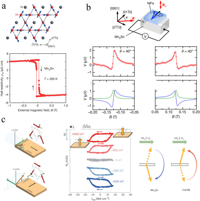
a Crystal and spin structure of Mn3Sn. The anomalous Hall effect of Mn3Sn was detected at room temperature. Adopted from ref. 21. b Schematic diagram of the spin-pumping measurement in the Mn3Sn/NiFe device. The measured voltage by spin pumping under positive and negative magnetic fields, respectively, indicating the magnetic inverse spin Hall effect. Adopted from ref. 112. c Schematic diagram of the spin-orbital torque induced magnetic state switching at different geometry. Schematic of the RH–I curves for the measurement geometry where injected spins σ are perpendicular to the magnetic easy plane. Schematic of the SOT switching of the octupole moment and the magnetization vector in Mn3Sn and CoFeB, respectively, showing the opposite switching polarities in the two systems. Adopted from ref. 103.
Above, magnetic solids conventionally fall into two fundamental phases—ferromagnets and antiferromagnets. Ferromagnets exhibit robust macroscopic magnetization, stemming from spin polarization in reciprocal momentum space. In contrast, antiferromagnets exhibit vanishing net magnetization, analogous to nonmagnetic materials. In conventional antiferromagnetism, compensatory antiparallel alignment of atomic magnetic moments in physical space results in the effective cancellation of atomic moments, leading to an extremely small macroscopic net magnetization. This implies the absence of a counterpart spin-polarization order parameter in reciprocal momentum space. Consequently, conventional antiferromagnets share similarities with nonmagnetic materials and remain undetected by macroscopic electrical or optical probes commonly effective in ferromagnets.
Recently, a third distinct and relatively abundant phase called “altermagnetism” has been established. This phase is characterized by compensated magnetic ordering in direct space with opposite-spin sublattices connected by crystal-rotation symmetries. The alternating arrangement of magnetic moments, stemming from a robust nonrelativistic origin, converges to a zero net magnetization as the relativistic spin-orbit coupling approaches zero. Furthermore, it exhibits a corresponding unconventional spin-polarization order in the reciprocal momentum space that reflects the same rotation symmetries, which displays a corresponding alternating order of spin polarization in reciprocal momentum space (Fig. 5a). This direct-to-reciprocal-space correspondence results in electronic band structures with time-reversal (({mathscr{T}})) symmetry and alternating momentum-dependent signs of the spin splitting104,105,106.
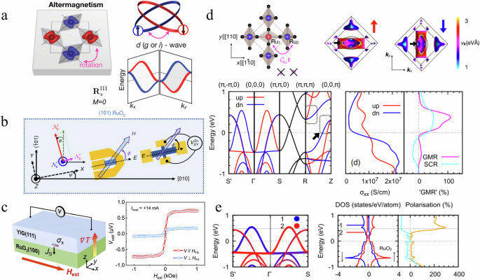
a Altermagnetic model with opposite-spin sublattices connected by rotation and not by translation or inversion, and corresponding distinct spin-group form, zero net magnetization, ({mathcal{T}})-symmetry breaking spin splitting with alternating sign, anisotropic sublattice spin densities, and anisotropic d-wave spin-split Fermi surfaces. Adopted from ref. 25. b Spin-torque ferromagnetic-resonance measurements for the sample schematics and definition of the coordinate axes for the (101)-oriented sample. Adopted from ref. 107. c The spin Seebeck effect of the RuO2/YIG(111) sample. Adopted from ref. 27. d First-principles calculations of the giant magnetoresistance (GMR) in RuO2. Adopted from ref.104. e First-principles calculations of the TMR in RuO2. Adopted from ref. 104.
Ruthenium dioxide (RuO2) is a conductive rutile oxide with a crystal structure belonging to space group (Pfrac{{4}_{2}}{m})nm, exhibiting a globally centrosymmetric arrangement (Fig. 5d). RuO2 is characterized as an antiferromagnet. A. Bose et al. 107 demonstrate that (101) direction of the collinear RuO2 generates a spin current with a well-defined tilted spin orientation, approximately parallel to the Néel vector (Fig. 5b). Moreover, spin-to-charge conversion originating from RuO2 through spin Seebeck effect measurements is observed27. The spin Seebeck voltage remains detectable even when the injected spin current is polarized along either the directions of the voltage channel or the thermal gradient (Fig. 5c), indicating the unconventional spin-charge conversion from the spin-splitting band structure. Besides, RuO2 displays band structures featuring Dirac nodal lines safeguarded by non-symmorphic symmetries. These nodal lines hold the potential to induce robust spin Hall effect (SHE). Beyond the SHE, RuO2 has garnered significant attention due to the discovery of anomalous antiferromagnetism108,109, crystal Hall effect24, and predictions of a magnetic SHE. And RuO2 has been associated with giant tunneling magnetoresistance (Fig. 5d, e), further enhancing its multifaceted properties and potential applications in diverse fields.
Moreover, the study of magnetic excitations provides crucial insights into the fundamental properties of different phases of matter and the applications of magnetic materials. Based on density-functional theory calculations, researchers observed that the THz-range magnon bands in RuO2 exhibit alternating chiral splittings73. Similar to the alternating spin splitting of electronic bands and possess linear magnon dispersion near zero wavevectors. This unconventional characteristic makes altermagnetic materials a promising material platform for spin caloritronics and magnonics.
Summary and outlook
Figure 6 summarizes the intriguing progress in quantum materials (TIs, TMOs, 2D, and (Alt)AFM materials) (inner circle), along with their characteristics, including advantages (middle circle) and disadvantages (outer circle). As discussed in Section II A, TIs are being explored to reduce the SOT switching current through spin-momentum locked topological surface states even at room temperature, providing an energy-efficient writing method for future MRAM technology. Meanwhile, the strongly correlated oxide materials with flexible control of symmetry and novel symmetry-breaking-induced spin-related effects are summarized in Section II B. Then, in Section II C, low-dimensional 2D van der Waals materials with magnetic orders open a new avenue for future high-TMR and scaling-down spintronic devices. Recent progress on novel unconventional antiferromagnets, such as non-collinear antiferromagnetic and altermagnetic materials with novel spin structures, bands, and transports, inspires opportunities for ultrafast spintronic devices as in Section II D.
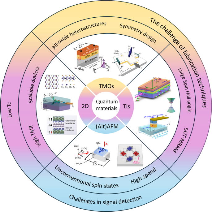
A schematic illustration of the intriguing research topics, applications, and characteristics of TIs, TMOs, 2D materials, and (Alt)AFM (inner circle), highlighting versatile ways to control the magnetic state and their advantages (middle circle) and disadvantages (outer circle). Adopted from refs. 14,25,46,47,58,96,112,113.
Integrating novel quantum materials into current CMOS circuits would be a crucial step towards practical applications, while challenges arise due to the distinct material fabrication methods for preparing specific quantum materials, such as TIs typically grown by MBE, and recently Mahendra DC et al. 11 achieved the growth of BixSe(1-x) with high SOTs at room temperature on thermally oxidized silicon substrates by magnetron sputtering which is compatible with CMOS industry; the wafer-scale 2D magnetic materials with uniform structural, magnetic, and electronic properties are needed for high-density spintronic applications. For AFMs, the efficient electrical detection and manipulation of AFM orders are major challenges for AFM-based spintronic applications, and recent works of antiferromagnetic tunnel junctions110,111 shed light on the future directions for AFM spintronics.
This review serves as a summary focusing on the latest advancements in the application of spintronics. Using SOT to separately control the read and write operations in magnetic storage devices is a technical approach. Apart from introducing quantum materials like topological insulators, transition metal oxides, two-dimensional materials, non-collinear antiferromagnets, and altermagnetic materials to enhance the performance of low-power spintronic devices, it is also needed to tackle various engineering and reliability issues when applying spintronic devices to practical applications. Exploring the applications of spintronic materials in logic devices and spin logic is essential to enable widespread industrial adoption of spintronics. With ongoing research into more quantum materials, we anticipate further improvements in the performance of spintronic devices, facilitating their future applications in magnetic memory, sensors, and logic technology.


Responses