Recent progress in spin-orbit torque magnetic random-access memory

Introduction: Value proposition of SOT-MRAM
The miniaturization predicted by Moore’s law has driven the evolution of electronic devices, leading to the explosive growth of our digital society as today1. However, as we continue to advance high-performance computing and energy efficiency, traditional charge-based memory technologies such as Static Random-Access Memory (SRAM) encounter significant challenges, primarily stemming from leakage current and limited density scaling, especially as the industry transition to the nanosheet transistor era1.
Magnetic random-access memory (MRAM), leveraging the spin properties of materials for data storage, has emerged as a promising solution to the challenges of charge-based memory devices2,3,4,5,6. At the core of MRAM is the magnetic tunnel junction (MTJ), a heterostructure comprising an oxide tunneling barrier sandwiched between the free and pinned layers. In MTJ devices, the magnetization state of the free layer serves to store bits of information, while the magnetization state of the reference layer remains fixed. Over the years, MRAM technology has seen significant advancements, boosting the scalability and performances2,3,4. With its non-volatility, fast read/write speeds, and high endurance, MRAM holds the potential to replace charge-based memory in various levels of the memory hierarchy (Fig. 1).

MRAM technologies provide promise to replace charge-based memory devices at different cache levels, ranging from L1 to L4. SRAM and DRAM stand for Static Random-Access Memory and Dynamic Random-Access Memory, respectively, while HDD refers to magnetic hard disk drives. SOT-MRAM is aimed at replacing SRAM due to its fast operation, while STT-MRAM is targeted for high-performance and high-density embedded DRAM applications. Voltage-controlled magnetic anisotropy technology offers potential for low-power operation and is being explored as a replacement for DRAM.
While Spin-Transfer Torque (STT)-MRAM has matured, its writing operation where a current is injected through the junction to switch the magnetization orientation of the free layer, faces inherent trade-offs between fast switching speeds and long-term endurance, primarily attributed to the shared read and write current paths2,4,5.
In response to these challenges, Spin-Orbit Torque (SOT)-MRAM, by employing separated write and read paths, has emerged as a promising alternative to mitigate the challenges associated with fast operation and high endurance in STT-MRAM devices5,7,8,9,10. This unique feature positions SOT-MRAM as a compelling candidate for providing a fast and dense memory alternative to SRAM (at least for the bigger caches), where high performance and reliability are important. Following the industrial trend towards chiplets and 3D integration, high-performance memory dies can be envisioned for 3D integration alongside accelerator processing units.
However, realizing the full potential of SOT-MRAM requires overcoming several critical hurdles such as:
-
Integrating perpendicular magnetic anisotropy (PMA) systems is imperative to unlock the scalability potential of SOT-MRAM, aligning it with the evolution of advanced technological nodes.
-
Implementing field-free switching mechanisms and achieving low switching currents in PMA systems are also critical for practical application of SOT-MRAM.
-
Furthermore, ensuring compatibility with back-end of line (BEOL) complementary metal-oxide-semiconductor (CMOS) fabrication processes is essential for seamless integration into existing manufacturing processes.
To address these challenges, advancements in understanding physics of SOT phenomena, materials research, and device engineering are essential for realizing SOT-MRAM technology. The fundamental physics of charge-to-spin conversion and methodologies for quantifying its efficiency across various material categories, along with SOT induced magnetization switching, have been comprehensively covered in numerous review articles5,9,10,11,12,13. In this review, our primary focus lies on the technological aspects, particularly enabling SOT-MRAM technology through material advancements and device integration strategies.
SOT-MRAM with in-plane MTJs have been demonstrated to be compatible with BEOL processes and enable field-free switching operation14,15. However, achieving further miniaturization and scaling of in-plane SOT-MRAM technology is hindered by specific elliptical shape requirements, limiting their scalability potential.
Therefore, this review delves into recent advancements in perpendicular SOT-MRAM device development, highlighting important technological requirements, progress of material research, large-scale integration demonstrations, and approaches for field-free SOT switching. Ongoing research endeavors aim to achieve BEOL compatibility, ultra-scale cells, and voltage-gated SOT devices in multi-pillar MTJs, thereby addressing the footprint challenges and prospects in SOT-MRAM technology.
Key requirements to enable SOT-MRAM devices
SOT-MRAM memory cell typically consists of a top-pinned 3-terminal MTJ where two contacts are connected to the SOT track for write operation while one to the top of the pillar for TMR read operation (Fig. 2). While this design leads to a larger footprint compared to 2-terminal STT-MRAM devices, it offers advantages in tunnel barrier integrity, potentially reducing writing errors and enhancing endurance5. Ongoing research includes alternative SOT device designs, such as multi-pillar cells with shared SOT layer, aiming to maximize cell density and performance16,17,18. This topic will be discussed later in this review.
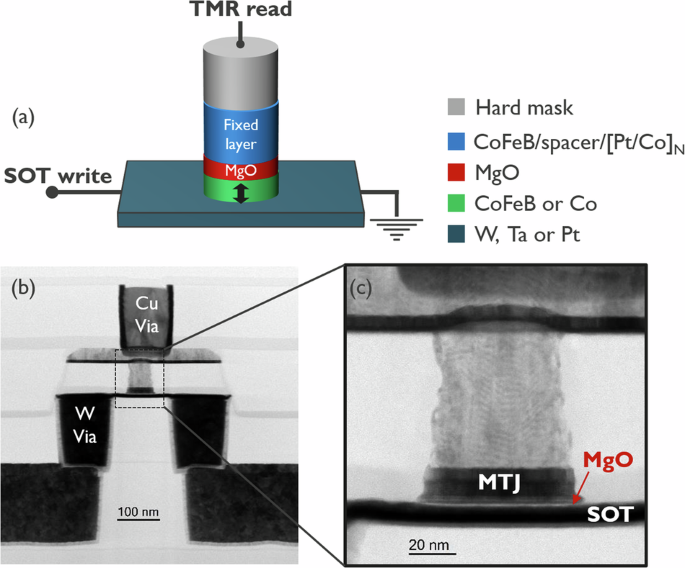
a Schematic of three-terminal SOT-MTJ devices illustrates the write operation enabled by charge current flow in the SOT track, inducing magnetization switching of the free layer, while read operations utilize electrical detection of TMR signal. b Transmission electron microscope images depict SOT-MTJ devices fabricated via CMOS-compatible processes on 300 mm wafers. W vias are used for applying current along the SOT track during write operations, while Cu vias serve for read operations. c High magnification image reveals MTJ cells with straight-profile free layers placed on continuous SOT tracks.
In SOT-MRAM, critical criteria for MTJ cells require energy efficient reading and writing of bit information while remaining compact and compatible with BEOL CMOS processes. These requirements are influenced by various factors like tunneling magnetoresistance (TMR), efficiency of charge-to-spin conversion, SOT track resistance, and thermal stability, impacting overall power consumption and performances5,9. The requirement of an external magnetic field for deterministic SOT switching in perpendicular MTJs adds an additional complexity to development of materials and processes.
Conventionally, perpendicular MTJ devices employ materials like CoFeB for both the free layer and reference layer to obtain high TMR ratios and high PMA. Using double MgO barrier concept developed in STT-MRAM technology to enhance thermal stability but this approach presents challenges for SOT-MTJs regarding the spin transparency at the interface between SOT track and free layer. An alternative hybrid free layer concept has emerged, enhancing thermal stability and enabling the introduction of complex materials19,20.
Additionally, the fabrication process of SOT-MRAM poses at least one extra challenge compared to its STT-MRAM counterpart. Indeed, precise control of the etch-stop process during MTJ pillar patterning step is crucial in preventing inadvertent damage on the thin (<10 nm) SOT track. Unlike established etching techniques in STT-MRAM, the integrity of the SOT layer requires a precise approach of etch-stop during the patterning process of MTJ pillar since minor deviations in etching process parameters can profoundly affect device performance and reliability [Fig. 3].
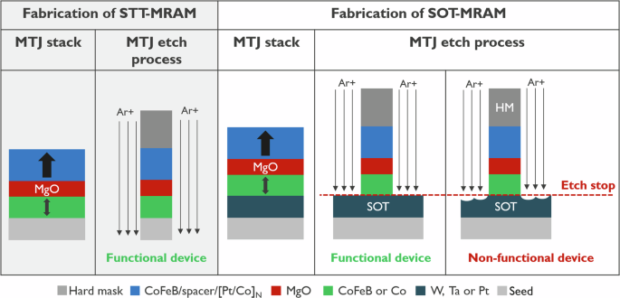
STT-MRAM devices allow over-etching through the seed layer, while the integration process for SOT-MRAM demands precise etch-stop on the tunneling barrier without surface damage to SOT track materials.
Material and device integration of SOT-MRAM
To advance the practical integration of SOT-MRAM devices, the selection of materials stack for both SOT and magnetic layers plays a crucial role in determining device performance metrics such as writing/reading energies, data retention and endurance. Hence, research and development of the SOT-MTJ stack involves addressing two key aspects:
-
1.
The SOT track material, which focuses on enhancing the charge-spin conversion ratio of damping-like torque to minimize write current.
-
2.
Optimizing the free layer to enhance MTJ properties such as TMR, PMA and compatibility with integration processes such as thermal budget at BEOL 400 °C annealing.
This section discusses critical aspects for optimizing SOT-MTJ performance to meet practical application requirements. It covers the materials used in SOT devices, including spin sources and magnetic free layers. Spin sources generally search for high charge-to-spin conversion efficiency, eventually resulting in low critical switching current11,12. The selection of magnetic free layers prioritizes compatibility with MRAM technology integration processes while ensuring MTJ properties meet requirement of high TMR and retention.
SOT track materials
Spin sources from heavy metals
The spin Hall effect (SHE) in heavy metals such as Pt, Ta, or W, owing to the strong spin-orbit coupling, is a phenomenon wherein a charge current induces the generation of a transverse spin current perpendicular to its flow direction. This phenomenon is the main driver for the development of SOT-MRAM technology. The key advantages of these materials are high spin Hall angles, integration-friendly process, in particular their compatibility with PMA magnetic layers5,11,12. Numerous studies have focused on optimizing these materials to achieve a high charge-to-spin conversion ratio while preserving the good PMA of the magnetic layer. In Fig. 4a–c, Kumar et al. revealed that undoped Tungsten (W) changes a β-to-α phase transition at ~4 nm, resulting in a loss of PMA and SOT efficiency21. Interestingly, they demonstrated that introducing oxygen (W(O)) or nitrogen (W(N)) doping extends the β-phase thickness, altering properties such as PMA and magnetization saturation while maintaining a similar intrinsic spin Hall efficiency (~−56%). Employing a W (O, N) bilayer lattice optimizes PMA and enhances anti-damping SOT efficiency, extending the critical thickness for phase transition and improving anti-damping SOT efficiency (-44.4% vs. -35%) compared to undoped W. This enhancement eventually reduces the threshold current for the switching of free layer by 25% when integrated into SOT-MTJ devices21.
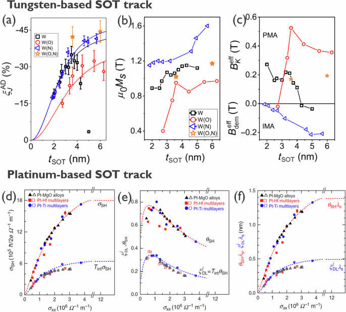
a Thickness dependence of anti-damping SOT efficiency (({{rm{xi }}}_{{rm{J}}}^{{rm{AD}}})) for various types of doped Tungsten. The solid lines represent fits to experimental data points using a drift-diffusion model to extract the intrinsic spin Hall angle and the spin diffusion length. b Saturation magnetization of Co-Fe-B plotted versus doped Tungsten layer thickness. c Effective anisotropy field (({{rm{B}}}_{{rm{eff}}}^{{rm{K}}})) of Co-Fe-B versus Tungsten thickness. Positive ({{rm{B}}}_{{rm{eff}}}^{{rm{K}}}) values indicate PMA while negative values correspond to in-plane magnetic anisotropy due to demagnetization field effects. Figure (a–c) are reprinted with permission from ref. 21, copyright 2021 by the American Physical Society. d The plotted figures illustrate the measured TintσSH (open symbols) and intrinsic spin Hall conductivity (σSH, solid symbols), (d) the spin Hall ratio (θ;SH, solid symbols), and (e) the damping-like SOT efficiency per unit current density (ξDL, open symbols). Additionally, (f) θ;SHλS and ξDLλS are shown for Pt-MgO alloys, Pt-Hf multilayers, and Pt-Ti multilayers, all plotted against electrical conductivity (ρxx). Figure (d–f) are reprinted with permission from ref. 26, copyright 2021 by the AIP publishing.
Additionally, intrinsic factors like crystal structure22, the orientation of crystal structure23, and film resistivity24,25 play key roles in modulating the SOT efficiency, enabling tailored material design for specific applications. Beyond traditional heavy metals, transition metals like Mo, Ru, Pd, and 3d metal Cr, despite weaker spin-orbit coupling, exhibit substantial SOT efficiency12. Furthermore, alloys with heavy elements such as CuAu, AuPt, PdPt, and TaPt offer unique advantages in SOT, with tunable spin Hall angles and resistivity12.
Platinum, noble among heavy metals, is distinguished by its substantial spin Hall conductivity, low resistivity, high thermal stability, and compatibility with CMOS processes. Recent works by refs. 26,27. have revealed a relationship between intrinsic spin Hall conductivity of Pt and longitudinal resistivity, demonstrating a strong, non-monotonic trend. Alloys of Pt with elements such as Au, Pd, or Cu enhance both longitudinal resistivity and spin Hall resistivity, thereby maximizing anti-damping torque, Fig. 4d–f. Consequently, these heavy-element alloys offer promising pathways for further advancement in SOT technology.
Topological insulator materials and beyond
In demand of pushing switching current to lower boundary, materials with high spin Hall angles like topological insulators (TIs), have emerged as promising candidates28,29,30,31,32. This is attributed to their high spin-orbit coupling, resulting in complete spin-momentum locking in surface states. Leveraging TIs for SOT-induced magnetization switching has shown ultra-low current density at room temperature28. While Bi2Se3, Bi2Te3, and BixSb1-x are standout choices, their deposition via molecular beam epitaxy presents challenges for industrial-scale production. Moreover, the high resistivity in TIs potentially challenges for low-power demands. Recent studies on magnetron sputtered TI films30,33 have shown promising results, achieving significant spin Hall angles and reduced resistivity. These advancements signify progress in exploiting the potential of TIs for SOT devices. However, challenges persist in integrating TIs into MRAM devices, including issues related to intermixing with ferromagnetic materials and susceptibility to processing damage. Therefore, research efforts are underway to enhance the thermal budget of TI materials, ensuring they meet the requirements above 350 °C in BEOL processes34,35.
Interestingly, by incorporating molybdenum (Mo) into TI/ferromagnet (FM) structures, Pan et al., have successfully grown high-quality CoFeB/MgO layers on epitaxial TIs34. The resulting TI/Mo/CoFeB/MgO film stack demonstrated robust PMA that withstands annealing up to 400 °C, meeting BEOL thermal budget requirements. Remarkably, this study demonstrated that the energy efficiency of TI-based structures is more than an order of magnitude greater than similar heavy metal-based structures. Therefore, the demonstrated current-induced magnetization switching, energy efficiency, and thermal tolerance in TI/Mo/CoFeB/MgO film stacks with PMA represent a significant step toward practical SOT implementation with TI materials.
It is worth to note that ongoing research continues to explore TIs and other materials like van der Waals compounds such as Dirac Weyl semimetals28,36,37,38. Indeed, Dirac and Weyl semimetals holds the potential in advancing SOT-MRAM technology, owing to their remarkable SOT efficiencies and distinctive electronic properties, enabling low-power and high-performance memory applications. Dirac and Weyl semimetals, characterized by their metallic nature, demonstrate efficient charge-to-spin conversion from both surface and bulk states, resulting in high SOT efficiency, making them as promising candidates for SOT-MRAM. Additionally, their lower resistivity compared to TIs holds promise for low-power SOT devices. Importantly, the low crystal symmetry in nonmagnetic Weyl semimetals generates out-of-plane spin polarizations, leading to unconventional out-of-plane damping-like SOT39,40. This capability enables field-free deterministic SOT-induced magnetization switching of PMA systems, streamlining their integration into established SOT-MRAM technology. Nevertheless, depositing the PMA magnetic layer directly onto Weyl semimetals remains challenging due to concerns about disrupting time-reversal symmetry and compromising topological properties. Maintaining high-quality crystalline films, addressing material defects, and integrating with CMOS technology also pose significant obstacles28. Despite these challenges, topological materials hold promise for revolutionizing MRAM technology. Enhancing material quality, interface engineering, and thermal stability while preserving scalable and cost-effective fabrication methods is crucial for the practical implementation of SOT-MRAM technology in commercial applications.
To address the thermal budget challenges of TI and Weyl semimetal materials, ongoing research is exploring a new class of topological semi-metals based on half-Heusler alloys, which offer a high spin Hall angle and improved thermal budget41,42,43,44,45,46. Crystal structure of half-Heusler alloy topological semi-metals materials is constructed from three kinds of element XYZ, where X and Y are transition or rare-earth metals, and Z is the main-group element. These materials offer high controllability of lattice constants and band structures41. Unlike TIs, half-Heusler alloy topological semi-metals have a cubic structure that matches FM materials and MgO-based tunneling barrier, and their high melting points ensure BEOL process compatibility. For instance, Shirokura et al. has recently demonstrated a giant spin Hall angle up to 4.1 and a thermal budget up to 600 °C with YPtBi42. Furthermore, magnetization switching of a perpendicular CoPt thin film using YPtBi-based SOT track has been demonstrated at significantly lower current densities than heavy metals. Although lower growth temperatures degrade the spin Hall properties of YPtBi, recent studies on YPtBi thin films deposited via sputtering at temperatures as low as 300 °C suggest that achieving giant spin Hall angle at lower temperatures is feasible45,46.
Further development is needed to demonstrate high SOT efficiency in perpendicular MTJs with YPtBi-based SOT tracks, particularly focusing on TMR and nanoscale implementation. Integrating YPtBi into nanoscale MTJ structures requires precise control over material deposition and interface quality to maintain the intrinsic properties of YPtBi and ensure high TMR and effective SOT efficiency. The challenge is to maintain high thermal stability and spin Hall efficiency at reduced dimensions, crucial for device scalability in practical applications. Overcoming these obstacles will enable the use of YPtBi’s superior spin Hall angle and thermal budget in advancing SOT-MRAM technology.
Impact of longitudinal resistivity on the performance of SOT-MRAM devices
In the writing scheme of SOT devices, electrical current flows along the SOT track to switch the magnetic state of the free layer. Therefore, the longitudinal resistivity of SOT materials plays crucial role in determining the writing power and performance of SOT-MRAM devices. Among various SOT materials, those with lower resistivity lead to reduced power consumption, enhancing the energy efficiency and overall performance of SOT-MRAMs25,47. For instance, by comparing switching efficiency of different SOT-based materials, Zhu et al. highlighted high SOT efficiency and low resistivity Au0.25Pt0.75-based SOT track outperforms other materials like Pt, β-W, and β-Ta, exhibiting significantly lower power consumption25. Additionally, materials with higher resistivity, such as TIs Bi2Se3 and (Bi, Se)2Te3, exhibit higher power consumption due to significant current shunting effects. Furthermore, benchmarking study by Li et al. showed that low resistivity of SOT track materials will significantly impact switching speed by reducing the overall resistance of the SOT track. This indeed leads to decrease the resistor-capacitor time constant of the circuit, eventually enabling faster switching times47. This enhancement is crucial for achieving higher operating speed, essential for improving SOT-MRAM performance and its competitiveness. Importantly, high resistivity can lead to increased Joule heating, impacting the thermal stability of the MTJ. Therefore, materials with lower resistivity, generate less heat, thereby enhancing thermal stability and reducing the risk of thermal degradation over time. This ensures long-term reliability in SOT-MRAM devices. Achieving a balance between resistivity and other material properties such as spin Hall angle is crucial for optimizing SOT-MRAM performance and mitigating parasitic effects, especially in advanced technology nodes.
In summary, heavy metals play an important role in the development of SOT-MRAM devices thanks to their high spin Hall angle, low resistivity, compatibility with PMA magnetic layers, and large-scale integration friendly. Doping techniques, as demonstrated with Tungsten, can optimize higher SOT efficiency. Platinum enhances anti-damping torque when alloyed with elements like Au, Pd, or Cu but the experimental demonstration high SOT efficiency in perpendicular SOT-MTJ with PtX-based SOT track has not been reported so far. Additionally, challenges exist with TI materials due to the integration with perpendicular MTJ integration and resistivity limitations, despite their potential for ultra-low switching current requirements. The half-Heusler alloy topological semi-metals offer potential for energy-efficient, BEOL-compatible SOT-MRAM devices due to their giant spin Hall angle and high thermal budget. Nonetheless, achieving high SOT efficiency in perpendicular SOT-MTJs with YPtBi-based tracks, focusing on TMR and nanoscale integration, requires further development. Ongoing research explores various materials for SOT applications, but mass production integration remains an open question.
Free layer materials on SOT track
Ferromagnetic materials with PMA such as Cobalt (Co) and cobalt-iron-boron (CoFe(B)) hold significant potential in the development of SOT-MRAM. They not only serve as key components for detecting and characterizing the SOT efficiency of heavy metals such as Pt and W11,12 but also commonly integrated in the free layer of MTJs. To accomplish a high TMR readout signal, CoFe(B) is often directly in contact with the MgO tunneling barrier due to its compatibility with the body-centered cubic (001)-oriented crystal structure of MgO. On the other hand, Cobalt is typically incorporated into the MRAM device through a hybrid free layer design19,20, which optimizes the performance of the device by mostly decoupling the “TMR” CoFeB part with a switching layer in contact with the SOT track.
In recent years, there has been considerable progress in leveraging antiferromagnets (AFM) and synthetic antiferromagnets (SAFs) for SOT-MRAM thanks to several advantages including the absence of stray fields, high thermal stability, and fast switching dynamics48,49. However, detecting magnetic states in nanoscale AFM and SAF devices still poses significant challenges due to their inherently low magnetic moments. Considerable advancement lies in the ability to manipulate the Neel order of AFM materials50,51 while the readout of magnetic state enabled via anisotropic magnetoresistance.
Interestingly, the recent breakthroughs in AFM writing52,53 and reading54,55 capabilities which highlight the remarkable potential of AFMs in boosting the performance of MRAM devices. These findings suggest that using AFMs as free and fixed layers for SOT-MRAM holds considerable promise. Indeed, AFM devices leverage the unique properties of the AFM Néel vector as a state variable, offering advantages over conventional FM materials, positioning them as ideal candidates for advanced spintronic devices. However, achieving complete electrical operation in a single AFM-based device remains significant challenges, include controlling Néel vectors in collinear antiferromagnet MTJs, where experimental demonstrations are lacking. Complex domain structures in AFM films hinder TMR signal, but aligning domains via FM layers may offer a solution56. Therefore, developing electrically driven methods to manipulate AFM domains is essential for future applications. Noncollinear AFM metals offer alternative energy efficient spin-torque switching but limited material options for suitable electrodes. Antiferromagnet MTJs with multiple anisotropy axes could enable multiple resistance states, while tunneling barrier choice and crystallinity are key for optimal performance. It is important to note that scaling effects from edge roughness during fabrication may impact nanoscale devices. Therefore, understanding and reliably controlling these effects at the nanoscale level is crucial for advancing antiferromagnet MTJs technology. Despite these challenges, antiferromagnet MTJs offer significant advantages over conventional MTJs in TMR, switching speed, and packing density, positioning their potential as a new spintronic device. Further research is essential to address these challenges and unlock the full potential of antiferromagnet MTJs.
It is worth to mention that SAFs are formed based on the Ruderman–Kittel–Kasuya–Yosida interaction, have also emerged as promising alternatives to ferromagnets in MRAMs. SAFs-based systems have been demonstrated to exhibit higher efficiency in SOT-induced switching compared to their ferromagnetic counterparts57,58,59,60 and have the option to integrate with CoFeB layer for TMR read-out19,61. Remarkably, recent breakthroughs in achieving deterministic SOT switching have shown the significant potential of SAF materials for SOT-MRAM technology62,63,64. Indeed, researchers have demonstrated field-free SOT switching solutions by reducing the Dzyaloshinskii-Moriya interaction at the interface between the heavy metal and magnetic layer57,58 or by introducing symmetry breaking through interlayer Dzyaloshinskii-Moriya interaction between magnetic layers65,66. These experimental results open a path to enable practical implementation of perpendicular SOT-MRAM devices with SAF materials.
Recent attention has focused on ferrimagnetic materials for fast switching dynamics, including rare earth-transition metal alloys like CoTb and GdFeCo67,68. These alloys exhibit bulk PMA and high SOT switching efficiency near the magnetization composition point. Ferrimagnetic Heusler alloy Mn2Ru1-xGa69,70 shares similar properties while insulating materials such as ferrimagnetic thulium iron garnet (Tm3Fe5O12) offer energy-efficient alternatives with comparable SOT switching efficiency to all-metal system71,72,73. Additionally, van der Waals materials have unveiled magnetic orders at the monolayer level, presenting novel opportunities for future explorations74,75,76.
In short, ferromagnetic materials like Co and CoFe(B) are vital for SOT-MRAM, offering efficient SOT detection and characterization while compatible with the state-of-the-art MTJs. Antiferromagnets and SAFs bring advantages such as zero stray fields and fast dynamics and higher SOT efficiency overcoming challenges of conventional ferromagnetic materials. Ferrimagnetic materials and insulators offer promising alternatives with efficient SOT switching, while van der Waals materials open new exploration paths at the monolayer level. It should be noted that a lot of these new materials suitability for integration will also be strongly influenced by their ability to withstand 400°C anneal thermal budgets without degradation, as it is a standard in advanced CMOS process flows.
Experimental demonstration of SOT-MTJ functionality
The integration challenges of SOT-MRAM pertain to preserving the integrity of SOT layer during the patterning process of MTJ pillars. Various studies have successfully demonstrated the functionality of SOT-MTJ devices in both PMA and in-plane systems. The utilization of various SOT track materials in these MTJ devices highlights the adaptability and versatility of SOT-MRAM technology. Table 1 provides experimental reports of SOT-MTJ devices along with their key characteristics. The first proof of concept for a perpendicular MTJ was reported in 2014, featuring a Ta/FeCoB/MgO/FeCoB-based stack on a Ta track77. The author demonstrated reliable switching of the CoFeB free layer with current pulses at 5 × 10¹¹ A/m² in the Ta layer.
In 2018, Garello et al., reported the first demonstration of perpendicular SOT-MTJs cells comprising W/CoFeB/MgO-based stack on 300 mm wafers using CMOS-compatible processes78. In this study, specific stop-etch conditions have been developed to leave the W layer intact while patterning the MTJ pillar without producing sidewall shorts across the MgO barrier. This study demonstrated promising characteristics of 62 nm SOT-MTJ devices with a TMR of 90% and reasonable high thermal stability. By evaluating both STT and SOT switching performances in the same device, the authors found that, in STT switching, the critical voltage is ~1 V (corresponds to switching energy ~470 fJ), while SOT achieves reliable switching at ~1 V within 210 ps and at 0.7 V within 500 ps, resulting in an energy as low as 350 fJ at 280 ps, respectively, Fig. 5. Additionally, endurance measurements on a 50 nm device show robustness, enduring up to 5 × 10¹⁰ events using 100 ns. The demonstration of SOT driven switching in perpendicular MTJs not only highlights the potential of SOT-MRAM technology but also signifies an advancement in exploring the SOT switching dynamics in nanoscale devices. By utilizing TMR signal detection, which provides a higher signal-to-noise ratio compared to conventional Hall bar detection methods, researchers can now delve deeper into the underlying physics of SOT switching at the nanoscale. This demonstration also opens new avenues for studying how nanofabrication processes impact the performance and reliability of these devices. Furthermore, by gaining insights into the effects of nanofabrication on device behavior, it allows us to refine fabrication techniques and optimize device designs for enhanced performance and functionality.
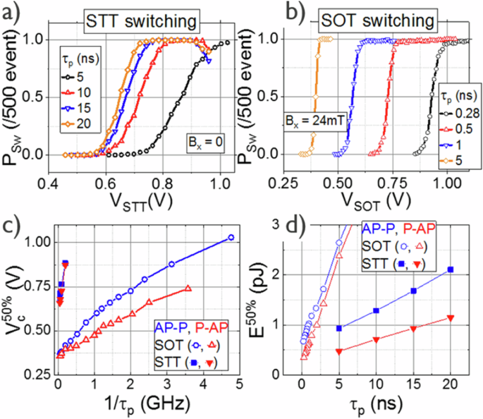
a, b The distribution of switching events is depicted relative to pulse voltage VSTT and SOT for different pulse durations τp (P-AP transition). c Critical switching voltage is shown as a function of the inverse of pulse duration, demonstrating switching frequencies up to 5 GHz. d Switching energy is illustrated over time, highlighting the ultrafast and low-power performance of SOT devices. The figure is reprinted with the permission from ref. 78, copyright 2018 by IEEE.
SOT switching dynamics in MTJs via real-time electrical detection
Understanding SOT-driven magnetization switching dynamics in nanoscale devices promises scalable, low-power, and high-speed operation of SOT-MRAM devices79,80. Through real-time single-shot measurements of SOT driven switching in MTJ devices, ref. 81, revealed deterministic and stochastic events in the switching process. The finding reveals the finite incubation time necessary for SOT-induced magnetization reversal, determined by the interplay of SOT, in-plane field, and Joule heating. Comparative analysis between SOT-induced reversal and STT in the same device highlights significant differences in dynamics, timescales, and efficiency of the two mechanisms. Fig. 6.
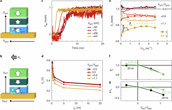
Schematics depicting SOT-induced switching are presented for the reference layer pointing both up (a) and down (b). Black arrows indicate bias, while white block arrows signify magnetization states. Yellow and red arrows represent the preferred switching directions due to SOT and STT, respectively. In (a), STT aids SOT-induced switching, whereas in (b), STT opposes it. c Averaged voltage-time traces of SOT-induced P-AP switching with varying STT biases are shown. d The critical voltage evolution is depicted as a function of pulse length for different VSTT/VSOT ratios. e Normalized critical voltages v ↑ and v ↓ are plotted as a function of inverse pulse length for various VSTT/VSOT ratio. f Change in average critical VCMA-like voltage contribution. The figures are reprinted with the permission from ref. 81, copyright 2020 by Springer Nature.
Further investigation distinguishes between the effects of STT and voltage control of magnetic anisotropy (VCMA) on SOT-driven magnetization reversal in MTJ devices.
In short, the demonstration of SOT-MTJ on 300 mm wafers marks a significant milestone in the development of SOT-MRAM. This achievement not only represents a technological advancement but also offers valuable insights into the fundamental aspects of SOT driven magnetization switching dynamics in nanoscale devices. The switching behavior observed in SOT-MTJ devices showcases reliable and efficient operation at sub-ns timescales. However, to fully exploit the benefits of SOT-MRAM technology, further research is required to address challenges related to optimizing reliable field-free switching mechanisms.
Field free SOT solutions with MTJ compatible
Role of damping-like and anti-damping torques on SOT switching
The damping-like torque effective field
In general, a SOT can be decomposed into two components: a longitudinal damping-like torque and a transverse field-like torque. The damping-like torque destabilizes the magnetization and induces rotation toward the spin polarization, leading to reversal, whereas the field-like torque drives magnetization into precession, impacting dynamics and switching speed5,9. Damping-like torque acts as an effective damping term, aligning magnetization with spin polarization and directly contributing to deterministic switching, making it more efficient. In contrast, field-like torque functions as an effective magnetic field, influencing precessional motion and affecting switching dynamics and speed. Understanding these mechanisms is crucial for optimizing SOT devices, highlighting damping-like torque for deterministic switching and field-like torque for overall performance. Currently, MTJ devices with PMA are designed as unit cells for SOT-MRAM due to their high thermal stability and scalability. In this device, the damping-like torque can immediately drive the magnetization into the in-plane direction and achieve switching in the presence of an external in-plane field to break symmetry, eventually determining the perpendicular direction of the magnet due to the in-plane effective field (both damping-like and field-like) from SOT. However, this requirement for an assistant field is a major obstacle for the industrial application. Therefore, achieving magnetic field-free SOT switching has become a key in realizing SOT-MRAM5,9.
The anti-damping-like torque
The anti-damping-like torque acts against the intrinsic Gilbert damping of ferromagnet and enabling field-free switching of PMA ferromagnets. The anti-damping-like torque comprises two components: the anti-damping and the field-like components. In this scheme, the anti-damping component destabilizes the magnetization, inducing the rotation of magnetization towards the spin polarization, thereby enabling deterministic switching. In contrast, the field-like component acts akin to an effective magnetic field, driving the magnetization into precessional motion and influencing the switching dynamics. Various strategies have been explored to generate anti-damping out-of-spin to advance the development of SOT-MRAM technology. First, the materials like WTe240, MnPd382, and interfaces such as CuPt/CoPt83 leverage the lack of lateral inversion symmetry in their crystal structure. Passing an in-plane current through these materials generates out-of-plane spin polarization, facilitated by their unique electronic properties and crystal symmetries, enabling efficient conversion of charge currents into spin currents with an out-of-plane polarization component.
Secondly, tri-layer structure incorporating an in-plane magnet layer beneath the non-magnetic metal layer like the in-plane CoFeB/Ti/perpendicular CoFeB system, the interfacial Rashba field induces spin precession, leading to the creation of an out-of-plane spin polarization component84,85,86. This field-free switching concept will be comprehensively reviewed in the next section. These approaches exploit material properties and interfacial effects to enable field-free SOT switching. Mastering these mechanisms is crucial for advancing MRAM, where efficient and reliable magnetization switching is essential.
In short, both damping-like torque and anti-damping like torque play crucial roles in the development of SOT-MRAM technology. It is worth to note that their role on SOT-induced magnetization switching dynamics can be quite different. For instance, a larger damping-like torque efficiency can lead to improved device performance, such as lower switching current while the unconventional out-of-plane anti-damping-torque enable deterministic field-free switching of a PMA ferromagnet. Both PMA and in-plane MTJs enable field-free switching through the anti-damping mechanism, yet they possess distinct characteristics. In-plane MTJs have been effectively integrated into SOT-MRAM, demonstrating sub-ns write speeds and compatibility with BEOL processes, facilitating field-free switching. However, challenges in specific elliptical shape requirements limit scalability and widespread adoption in future memory applications. Perpendicular SOT-MRAM, on the other hand, shows promise for scalability and competitiveness in the memory market. Despite this, it faces practical hurdles due to the need for an external in-plane magnetic field to achieve deterministic SOT-induced magnetization7,8. Various strategies for enabling field-free SOT switching have been actively researched13,87. This involves introducing in-plane stray fields88, exchange bias89,90, lateral structural symmetry breaking within the device structure, typically achieved by incorporating a wedge-shaped layer or manipulating the geometry of the magnetic layer87,91,92. However, reproducible fabrication of a wedge layer remains a significant challenge, especially for large-scale wafer integration. Despite recent advancements, the demand for reliable field-free switching solutions remains pressing in SOT-MRAM technology. Additionally, current experiments and physical understanding are typically limited to Hall bar devices at microscale devices, limiting its capabilities to real application of SOT-MRAM devices. Furthermore, scaling effects resulting from edge roughness during fabrication processes may affect the field-free switching at nanoscale devices. Therefore, understanding and reliably controlling field-free switching at the nanoscale level in MTJ devices represents a crucial step toward advancing SOT-MRAM technology. This section will discuss experimental demonstration for field-free SOT switching manufacturable and compatible with perpendicular MTJs.
Stray field from magnetic hard mask
Garello et al. demonstrated an integration-friendly approach by embedding a Cobalt ferromagnet in the hard mask used to shape the SOT track during device fabrication process. This Cobalt magnetic hard mask generates an in-plane stray field large enough to induce symmetry breaking to enable field-free switching88, panel (a) in Table 2. The results show that devices exhibit sub-ns switching down 300 ps, without compromising MTJ properties. Endurance tests reveal a low write error rate of 105 events and endurance up to 1011 cycles at 1 ns, with negligible variation in SOT and MTJ resistances post-testing, confirming the robustness of the devices under high stress conditions. Real-time single-shot measurements revealed a stochastic incubation delay near the critical voltage threshold with a transition time of ~1 ns93. Importantly, this study emphasizes the negligible impact of magnetic hard mask on the MTJ properties.
In short, magnetic hard mask solutions offer advantages in manufacturable contexts but it also holds a set of challenges that potentially hinder their widespread adoption within SOT-MRAM technology. The first one lies in the scaling of cell size, where the stray field may diminish as the dimension of individual cells decreases. The second challenge is anticipated to be challenge for the integration of multi-pillar devices commonly used in high-density SOT-MRAM architectures. In this configuration, the stray field approach may not scale effectively to accommodate the increased density of memory cells.
Combination of STT + SOT for field-free switching
Recently, a full electrical control of field-free switching scheme in perpendicular SOT-MRAM devices has emerged, integrating both STT and SOT effects within a single device, panel (b) in Table 2. This approach offers two distinct scenarios: SOT assisting STT and vice versa. Through experimental validation and modeling, it has been shown that this combined approach enables various switching regimes. High SOT current enables fast field-free switching while low SOT assists STT dynamics, reducing incubation time94,95,96. Remarkably, this approach has been experimentally validated, demonstrating field-free switching without compromising sub-ns writing and endurance97,98. The combination between SOT and STT offers multiple advantages, including breaking the symmetry of SOT by even small STT currents. Furthermore, micromagnetic simulations illustrate the scalability of this method, with reduced power consumption by a factor of 10 as device size decreases from 60 nm to 10 nm.
In summary, the concept of combining STT and SOT certainly introduces an intriguing possibility for a full electrical control of field-free switching in perpendicular MTJ devices. However, it also raises concerns regarding the potential impact on device reliability, akin to the issues observed in STT devices. The reliability of such SOT devices, particularly concerning their endurance, needs thorough investigation. Evaluating how the current flow affects the tunnel barrier and endurance will be crucial in determining the feasibility and reliability of this field-free switching scheme.
Design of bending structure for field free switching
Recently, an innovative approach for field-free switching in perpendicular MTJs has been experimentally demonstrated by introducing a geometric bending structure of the SOT channel99, panel (c) in Table 2. This design introduces a structural imbalance within the system, prompting the flow of non-uniform charge current along the SOT channel. As a result, the modifications in spin current distribution led to non-uniform SOT exerted on the free layer of the MTJ, thereby breaking the time-reversal symmetry crucial for deterministic SOT switching. Micromagnetic simulations reveal that domain wall nucleation primarily occurs at the inner corner of the bent structure due to higher spin current density, influencing domain wall dynamics. This study found that factors like stray fields and Oersted field from the curved SOT channel minimally impact switching dynamics, while variations in damping parameters and Joule heating show moderate effects on switching reliability. Shortening the SOT channel is proposed to reduce resistance and enable studies with shorter pulse regimes. Additionally, a design-to-technology co-optimization (DTCO) analysis reveals that optimizing the MTJ position, closer to the inner corner, reduces switching current by ~32% while maintaining area efficiency. However, the implementation of device concept raises concerns regarding the occurrence of local Joule heating within the free layer. This design also poses challenges, particularly in terms of the large footprint resulting from the specific geometry of the SOT track. Additionally, there are implementation issues to be addressed, particularly in the context of multi-pillar devices, to enable high-density capabilities of SOT-MRAM devices.
Concept of hybrid spin source for field-free switching
Recent advancements have shown field-free switching in PMA systems by incorporating an in-plane magnet layer beneath the non-magnetic metal layer, forming a hybrid spin source layer derived from the bottom magnetic layer or its interfaces84,85,86,100,101,102,103,104. In this concept, the interface between a FM and a non-magnetic (NM) layer generates significant spin currents when a charge current flows into the FM/NM bilayer. This induces interface scattering driven by the spin-orbit field (BSO), triggering two key mechanisms: spin-orbit filtering and spin-orbit precession. Spin-orbit filtering selectively transmits or reflects spins parallel or antiparallel to BSO, resulting in a spin current polarized along BSO, while spin-orbit precession produces an out-of-plane spin polarization perpendicular to the magnetization direction of FM layers103,104. The FM/NM bilayer configuration generates spin currents with both in-plane and out-of-plane components, enabling sub-ns field-free switching with significantly reduced current densities102. Micromagnetic simulations highlight the critical role of the out-of-plane spin current in reducing the current density for short current pulse. Analysis reveals that the incubation time for field-free switching is orders of magnitude smaller than that observed in STT-driven switching. Recently, this field-free switching concept has been successfully demonstrated in multi-pillar (MP) SOT-MTJs devices, fabricated on CMOS-compatible 300 mm wafers105. Ultrafast field-free switching has been achieved using current pulses as short as 0.3 ns, with a corresponding power consumption of 60 fJ/bit.
In summary, hybrid spin sources using an in-plane magnetic layer within the structure offers a scalable solution. However, this approach also comes with its challenges including the shunting current passed into the underlying in-plane magnetic layer. Furthermore, the torque exerted by the SOT applies to both magnetic layers in the structure which potentially induces a reversal in the orientation of the in-plane ferromagnet. Such unintended reversals can introduce errors in the writing process, leading to higher write error rate and decreased overall reliability of the device.
Toward practical applications of SOT-MRAM
SOT-MTJ stack design for 400 °C BEOL compatible
The integration of SOT-MRAM technology into BEOL processes, compatible at annealing temperatures up to 400 °C, marks a significant advancement towards practical applications. However, this achievement holds a set of challenges including material intermixing at the interfaces. Honjo et al. has tackled these challenges by developing a canted SOT device, fully compatible with the 400 °C thermal tolerance requirement14. These achievements highlight the potential of canted MTJs design but the scalability challenges remain.
Additionally, employing interfacial PMA of CoFeB/MgO-based stacks at high annealing temperatures introduces complexities due to diffusion phenomena, potentially compromising the PMA interface.
In response to these challenges, a hybrid free layer design for BEOL compatible at 400 °C annealing with perpendicular MTJs has been demonstrated20. This stack design incorporates CoFeB for enabling high TMR read-out with intrinsic PMA material in contact with the SOT track, enabling retention control and improved thermal budget requirement, Fig. 7.
Comparison of single CoFeB free layer (a) vs the hybrid free layer stack design (b) which enable back end of line compatibility at 400 °C annealing while simultaneously enable high TMR readout and data retention. c Illustration of data retention (∆) versus size indicates achieving ∆ > 100 kBT down to 50 nm CD using the hybrid free layer. d The relationship between switching voltage (top) and current (bottom) versus the inverse of pulse width is demonstrated. Figure are reprinted with the permission from ref. 20, copyright 2021 by the Japan Society of Applied Physics.
Moreover, this concept holds potential to employ alternative magnetic materials on the SOT track while maintaining MTJ properties, providing flexibility in the SOT material set to further enhance device performance.
Experimental results demonstrated that retention of hybrid free layer design exceeding ∆>75 kBT down to a 50 nm size and operation at temperatures up to 125 °C. Endurance tests reveal robust performance of hybrid free layer devices under 2.1010 cycles with 1 ns pulses, indicating minimal degradation. Additionally, tight distributions of TMR and SOT track resistance across 300 mm wafers highlight the manufacturing potential and reliability of the hybrid free layer design. This advancement represents a significant step forward in the development of SOT-MRAM technology.
Enable ultra-scale SOT-MRAM cells to be compatible with smaller access transistors
Advancements in CMOS technology enable smaller access transistors, enhancing speed, efficiency, and density but providing lower operational currents for embedded MRAM. Consequently, downsizing of MTJ is imperative to be compatible with advanced node but poses a challenge due to compromised data retention106,107.
In response, Van Beek et al. have experimentally demonstrated alternative approaches to scale down both SOT tracks and MTJ dimensions, achieving scalability and compatibility with CMOS technology108. The authors demonstrated that scaled devices where the size of SOT track is comparable with size of MTJ reduces switching energy by 63%, reaching down to 79 fJ, Fig. 8. This leads to a significant improvement of write error rate performance, achieving a level of 10−5 while the endurance reached beyond 1015 cycles. Furthermore, using a BEOL compatible 400 °C hybrid free layer stack design addresses the challenge of scaling MTJ size while maintaining good data retention. While the W/CoFeB stack lacks sufficient retention for CD < 60 nm, the hybrid free layer stack exhibits higher retention (>100 kBT) down to 54 nm, allowing extended scaling. Shrinking the MTJ size to ~20 nm while maintaining retention requirements could reduce switching current to ~100 μA. This scaling approach offers significant advantages in reducing SOT-MRAM cell dimensions.
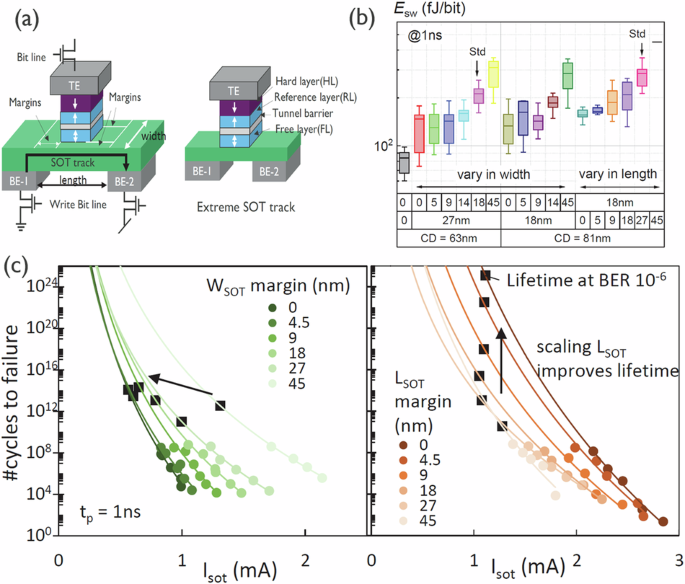
a An extreme SOT design with no margins is proposed to prevent power consumption within these margins. b Illustration of energy consumption (ESW) of devices with varying margins in width or length. The extreme devices exhibit the lowest ESW at 79 fJ/bit. c Endurance measurements conducted for 50% lifetime analysis using bipolar pulses under SOT stress for (left) various track widths with MTJ CD = 63 nm and (right) track lengths with MTJ CD = 81 nm. Figure are reprinted with the permission from ref. 108, copyright 2023 by IEEE.
High density and low power with Vg SOT concept
The 3-terminal configuration of SOT-MRAM devices requires the incorporation of at least two transistors, thereby posing challenges for high-density capability. To tackle these challenges, novel device concepts such as two terminal SOT-MRAM device109,110 and the concept of voltage-gate assisted (VGSOT-MRAM)16,17,18,111,112 has been proposed and experimentally demonstrated. The two-terminal SOT-MRAM aims to enhance density by reducing the number of terminals, while the VGSOT-MRAM leverages both SOT and VCMA effects to enable multiple MTJ pillars in the same SOT track. The VGSOT-MRAM device concept, the SOT is primarily responsible for enabling the switching of free layer while VCMA effect modifies its magnetic anisotropy. Incorporating VCMA effect offers benefits such as lower write currents for SOT switching and the potential for selective write operation in multi-pillar cell structures, addressing density limitations in conventional SOT technologies.
Concept of a two terminal SOT-MRAM devices
The 3-terminal configuration of SOT-MRAM increases cell size, challenging the competitiveness of SOT-MRAM in high-density applications. To address this, Sato et al. proposed and experimentally demonstrated the function of a two-terminal SOT-MRAM cell with a perpendicular MTJ, comprising a CoFeB/MgO MTJ pillar on an ultrathin Ta underlayer109. In this device configuration, the application of voltage generates both out-of-plane and in-plane currents where the out-of-plane current induces STT while the in-plane current induces SOT. The author demonstrated that the switching process was dominated by SOT as evidenced by symmetric switching depending on the applied in-plane field direction. Although STT only contributes around 10% to the switching process, the writing current for the two-terminal device is notably reduced by about 70% compared to purely STT-driven switching, suggesting higher energy efficiency compared to its STT-driven counterpart. This proof of concept highlights the potential for advancing simpler, high-density, and energy-efficient SOT-MRAM technology. Its simpler design enables higher-density memory arrays by minimizing connections and space requirements compared to standard SOT-MRAM devices. However, the development of two-terminal SOT-MRAM faces challenges, notably the high resistance issue arising from the series-connected SOT layer, potentially compromising reliable TMR readout. Addressing this requires exploration of low-resistivity SOT materials and novel structural designs to minimize resistance contributions from the SOT layer. Additionally, the requirement of an in-plane external magnetic field for SOT switching complicates device complexity, requiring further investigation into field-free SOT switching solutions. Concerns over device reliability emerge from the need to pass high current through the tunnel barrier of MTJ cells for write operation. Therefore, thoroughly investing the reliability of SOT devices, especially regarding endurance, is crucial. This involves assessing how current flow affects the tunnel barrier and endurance to determine the feasibility and reliability of this device concept.
Selective operation of multi-pillar SOT-MTJs devices via VCMA assisted SOT switching
Wu et al. developed a methodology to characterize voltage-gate assisted SOT effects on perpendicular MTJ devices with a W/CFB/MgO-based stack113, Fig. 9. The study showed a linear relationship between gate voltage and SOT write current, leading to a 25% reduction at Vg = 1 V. As a result, this led to a substantial decrease in total energy consumption with energy per bit reaching as low as 30 fJ for 80 nm devices at a speed of 400 ps. Additionally, reliability assessments showed write error rate down to below 10−5 and robust endurance exceeding 1012 cycles without degradation.
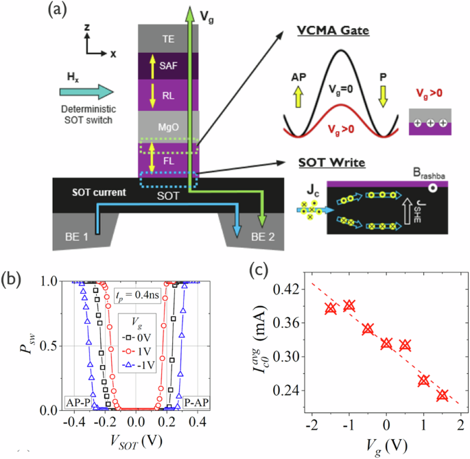
a A positive VCMA top gate induces electron accumulation at the FL/MgO interface, reducing the PMA of the FL and enabling SOT switching with reduced current. b Probability distribution of SOT switching (Psw) plotted against SOT pulsed voltage (VSOT) for various gate values (Vg) at tp = 0.4 ns. c Average intrinsic critical current (Ic0 avg) depicted as a function of Vg. Figure are reprinted with the permission from ref. 113, copyright 2021 by the American Physical Society.
Remarkably, Cai et al. have made significant progress on the development of VG SOT-MRAM concept by introducing multi-pillar MTJs on CMOS-compatible 300 mm wafers, showcasing lower write currents and enhanced integration density18, Fig. 10.
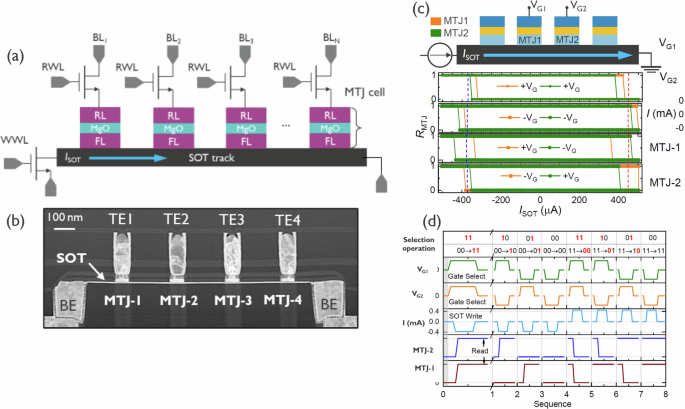
a Diagram illustrating the architecture of multi-terminal MTJs on a common SOT track. b Cross-sectional transmission electron microscopy (TEM) view of the integrated multi-pillar SOT device with four MTJ pillars. Separate top electrodes (TEs) enable individual voltage control and readout of the MTJs. c Diagram of the multi-pillar measurement setup and the switching loops for all combinations of ±VG (±0.5 V). d Experimental validation of selective operations on two bits. Sequential operations include MTJ initialization, input settings (gate voltages, and SOT writing current), and output readings (MTJ readout). Figure are reprinted with the permission from ref. 18, copyright 2022 by IEEE.
In this study, the authors showed that gate voltages enable individual selection of multiple MTJs on a shared SOT track, switched independently by sub-ns pulses, resulting in 30% reduction in operational current. This selective operation concept, requiring less transistors and lower writing energy, promises significant advancements in SOT-MRAM density and energy efficiency. Specifically, they also demonstrated successful selective switching of two bits, preserving magnetization states of unselected pillars via gate voltage.
Interestingly, Li et al. demonstrated the field-free switching VGSOT switching in IrMn-based perpendicular MTJs using MTJs with 80 nm diameters114. Experimental findings revealed field-free switching under various pulse widths and gate voltages, showcasing versatility and robustness of this device concept. Applying a gate voltage of 0.8 V led to a remarkable 70% reduction in critical current density, resulting in a 91% decrease in total power consumption. This result highlights significant energy consumption reductions with voltage-gated SOT switching, enhancing device efficiency. Endurance tests demonstrated over 1 × 10¹² write cycles and a low write error rate below 8 × 10⁻⁵, emphasizing device robustness.
Design-to-technology co-optimization analysis on voltage-gated SOT-based memory
The DTCO study suggests that a VGSOT design with multi-pillar MTJs can substantially reduce effective area compared to conventional SOT-MRAM, making it comparable to STT-MRAM and less than 50% of HD-SRAM, with minimal performance degradation115,116,117. Despite current limitations arising from high MTJ resistance, optimization strategies target improving read performance by optimizing the resistance-area product without compromising VCMA gate effects. Furthermore, write power remains higher for 2MTJ and 4MTJ designs compared to typical SOT cells due to increased SOT channel length and resistance. However, improvements in SOT and VCMA efficiencies are expected to significantly reduce switching current. The projection of VGSOT performance under specific conditions demonstrates significant improvements in read latency and write power, promising high-performance, low-power, and high-density SOT-MRAM memories, Fig. 11.
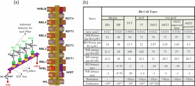
a Diagram and layout of a multi-bit SOT device. b DTCO analysis of performance across various embedded memory technologies at the 5 nm technology node (with VDD = 0.7 V). Figure are reprinted with the permission from ref. 18, copyright 2022 by IEEE.
In summary, while conventional 3-terminal SOT-MRAM faces integration complexities and high write currents, recent experimental advancements in VGSOT-MRAM offer promising solutions. By integrating SOT and VCMA effects, this hybrid device concept achieves remarkable reductions in write currents, leading to lower energy consumption and improved endurance. Multi-pillar SOT-MRAM architectures and field-free switching VGSOT switching techniques further enhance efficiency and reliability. Challenges persist, particularly in improving VCMA coefficient and SOT efficiency for enlarging the selective writing window. Moreover, DTCO analyses project significant improvements in effective area and performance for VGSOT-4MTJ designs, supporting the feasibility and scalability of VGSOT-based memory solutions. Thus, VGSOT-MRAM presents a pathway for next-generation memory applications, with the potential to overcome integration hurdles and improve energy efficiency for low-power, high-density SOT-MRAM technologies.
Perspectives and current challenges of SOT-MRAM
SOT-MRAM presents a significant promise in revolutionizing memory technology, offering sub-ns operation, practically unlimited endurance, and reasonable power consumption. We reviewed recent material research advancements, focusing on optimizing charge-spin conversion efficiency and field-free switching concepts, crucial for MTJ technology and BEOL processes compatibility. The proof of concept of multi-pillar MTJs with selective write operation using voltage-gated SOT devices hold potential in reducing switching currents and boosting memory density. Coupled with the development of ultra-scale SOT-MTJ cells, these advancements enhance device performance and energy efficiency.
Fabricating SOT-MRAM has posed significant challenges compared to STT-MRAM, particularly in controlling the integrity of SOT materials. However, the successful demonstration of SOT-MTJ on CMOS-compatible 300 mm wafers marks a significant milestone, offering valuable insights in SOT-driven magnetization switching dynamics in nanoscale devices and accelerating material research for more energy-efficient materials. Despite these advancements, realizing the full potential of SOT-MRAM requires overcoming challenges such as reliable field-free switching and low switching current.
We discussed various field-free switching schemes demonstrated experimentally in perpendicular MTJs. While magnetic hard mask solutions showed potential, integrating them faces hurdles, especially in scaling cell size. Stray field generation from magnetic hard mask may not scale for multi-pillar devices in high-density SOT-MRAM architectures, limiting memory density. Using current flow through the tunnel barrier in STT and SOT field-free switching scheme is intriguing but raises reliability concerns. Therefore, the reliability of this writing scheme, especially their endurance, requires careful investigation. Assessing the impact of current flow on tunnel barriers and investigating degradation mechanisms are vital for determining feasibility and reliability in this field-free switching schemes.
The bending current concept enables deterministic field-free switching in scaled SOT-MTJs, offering scalable, independent of material properties and compatible with wafer-scale manufacturing. However, it raises concerns about local Joule heating in the free layer. Challenges include the large footprint due to the geometry of SOT track and implementation issues in multi-pillar devices. Finally, unconventional out-of-plane spin with an in-plane magnetic layer below SOT track provides a scalable and energy-efficient solution but presents significant challenges. The risk of unintended reversals of in-plane magnet due to SOT-induced torque underscores the importance of optimization for reliable operation.
Advancing SOT-MRAM technology towards practical application, we discussed hybrid free design for 400 °C BEOL compatible with perpendicular MTJs, incorporates CoFeB for high TMR read-out and intrinsic PMA material, allowing for retention control and improved thermal budget requirement. Furthermore, simultaneously downsizing SOT tracks and MTJ dimensions via geometrical design was experimentally demonstrated to reduce the switching energy. Importantly, this advancement makes SOT devices to be accessible with small transistors at advanced technological nodes, to reduce switching current and energy while improving write error rate performances. Additionally, selective multi-bit write operations using VGSOT-MRAM concept offered significant advancements in density and energy efficiency. This device concept highlights the efficacy of voltage-gated SOT switching for high efficiency and integration density in multi-bit SOT devices, suggesting future research directions to enhance the density and performances of SOT-MRAM applications.
In summary, recent advancements in material research for SOT-MRAM focused on improving charge-spin conversion efficiency and reliable field-free switching mechanisms. These advancements are pivotal to ensure seamless integration with MTJ technology and manufacturing BEOL processes.
However, significant challenges persist in achieving a single device that combines low switching current, reliable field-free switching, and compatibility with BEOL processes. Addressing these challenges is crucial for unlocking the full potential of SOT-MRAM technology. Future research should prioritize refining reliable field-free switching schemes and reducing SOT switching current to drive SOT-MRAM technology evolution. These efforts will enhance efficiency, increase integration density, and broaden applicability in computing and memory systems.
While the focused topic of this manuscript is SOT, it is worth to mention the importance of ongoing research on orbital Hall effect to further improve the performance of spintronic devices118,119. Orbital Hall effect generates an orbital current perpendicular to an applied electric field through nonequilibrium interband superpositions of Bloch states induced by the field, transferring angular momentum from the lattice to the electron system. While detecting orbital currents experimentally remains challenging, recent theories suggest their potential to exert torque on magnetization in bilayer systems, potentially enhancing SOT device efficiency. Exploring orbital torque shows promise for enhancing spintronic devices, including MRAM, due to its unique characteristics and compatibility with various material systems. Its long-range angular momentum transport surpasses the limited spin transport length in metallic FMs, paving the way for applications beyond magnetization switching in MRAM. The extended decay of orbital currents hints at their potential for signal transmission among diverse array components. Additionally, the compatibility of orbital torque with different material systems encourages the exploration of novel device architectures and material combinations. While still in its early stages, the exploration of orbital torque in MRAM presents a compelling avenue for further research and development, given its unique advantages and potential synergies with existing spintronic concepts.


Responses