Recent progress on controlling spin-orbit torques by materials design
Introduction
The manipulation of magnetization is a critical aspect of spintronic research1,2,3,4, driving development of spintronic devices for information storage5,6,7,sensing8 and processing applications9,10,11, such as magnetic random-access memory (MRAM)12,13,14,15,16,17,18, nano-oscillators19,20,21,22,23,24,25, neuromorphic computing devices26,27,28,29,30, magnetic sensors8,31,32,33,34, and so on. Previously, Oersted field generated by charge current and current-induced spin transfer torque (STT)35,36,37 were employed to manipulate magnetization. In recent years, current-induced spin–orbit torques (SOTs)38,39,40,41 emerged as a more effective approach for manipulating magnetization. SOTs can be generated via various mechanisms, such as spin Hall effect (SHE)42,43,44,45,46, Rashba–Edelstein effect47,48,49,50,51,52, orbital Hall effect53,54,55,56,57,58, magnons59,60,61,62,63,64,65,66 and spin swapping67,68,69,70. In the case of spin Hall effect, an in-plane transverse charge current in the spin source materials generates a longitudinal pure spin current, which transports spin angular momentum with polarization ({boldsymbol{sigma }}) into adjacent ferromagnetic(FM) layer, exerting torques on the magnet. As for Rashba–Edelstein effect, spin accumulation is created by a charge current in a two-dimensional electron gas with SOC and magnetic exchange, exerting torque on adjacent magnetization. The produced spin–orbit torque could be decomposed into two components that are perpendicular to each other, a anti-damping torque ({tau }_{{AD}},{boldsymbol{propto }}{bf{m}}times {boldsymbol{(}}{bf{m}}times {boldsymbol{sigma }}{boldsymbol{)}}) and a field-like torque ({tau }_{{FL}},{boldsymbol{propto }}{bf{m}}times {boldsymbol{sigma }}), where ({bf{m}}) is the unit vector of the magnet6,13,38. To evaluate the charge-to-spin efficiency of a spin source material, the merits of figure, spin Hall angle (SHA) ({theta }_{{SH}}) is defined as6,13,38
where ({j}_{c}) is the charge current density in the spin source material, ({j}_{s}) is the generated spin current, (e) is the electron charge, and (hslash) is the reduced Planck constant. Considering that spin scattering and spin loss during the transportation could reduce the amount of spin angular momentum that arrives the adjacent ferromagnetic layer, another index SOT efficiency ({theta }_{{SOT}}) is used, which is defined as
where ({{rm{theta }}}_{{SH}}) is the SHA, and ({T}_{mathrm{int}}) is the spin transparency71,72,73.
SOTs offer several advantages on manipulating magnetization compared to STT6,74. Firstly, benchmark SOT materials show higher charge-to-spin conversion efficiency, which results in lower power consumption in the SOTs-based devices6,74. Secondly, the configuration of SOT devices are three-terminal structures with separate paths for writing and reading, giving arise to longer duration1,2,3,4,5,6. Thirdly, SOT materials are not limited to ferromagnet(FM), they also include ferrimagnets75,76,77,78 and antiferromagnets79,80,81,82 opening up new possibilities for novel spintronic devices.
To date, plenty of materials are identifed as capable of generating significant SOTs, including heavy metals(HM)38,39,40,76,77, oxides83,84, topological semimetals(TSM)85,86 and topological insulators(TI)87,88,89,90,91,92. However, acquirng SOT materials with larger SOT efficiency and electronic conductivity for energy-effiecient application is still challenging93,94,95. In addition, since out-of-plane magnetization is preferred in application due to its good miniaturization, deterministic switching of the out-of-plane magnetization is essential, which can be realized through SOT generated by z-polarized spin current39,40,95,96,97,98,99,100. However, this unconventional SOT is generally prohibited by mirror symmetry in common spin source materials, and symmetry breaking is required for generating SOT. To address these two challenges, researchers have developed strategies for controlling both the magnitude and polarization of SOTs through materials engineering. These strategies include: (1) Strain engineering of the spin Hall angle, (2) Interfacial engineering of the spin transmissivity and topological surface states, and (3) Symmetry engineering to achieve deterministic field-free switching of out-of-plane magnetization (see Fig. 1). In this review we aim to focus on recent research works that control SOTs by the above methods.
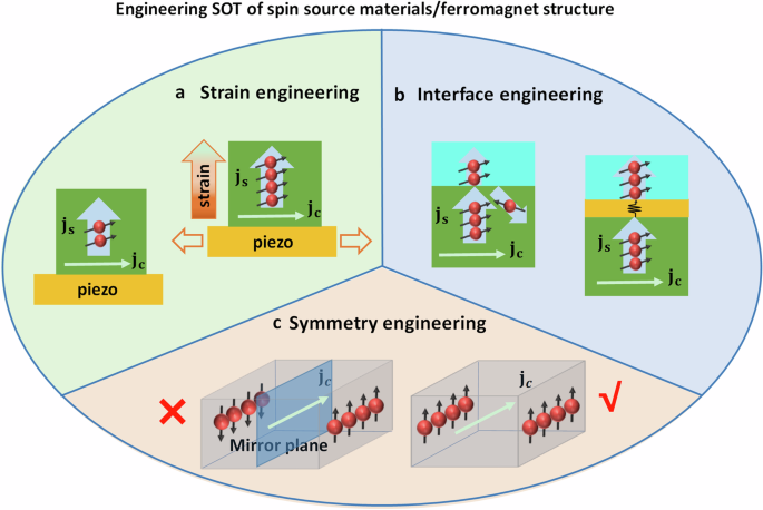
a Strain engineering. Application of strain from the piezo substrate onto the film enhances the spin current. b Interface engineering. Inserting an oxide layer into the spin source/FM structure increases the transparency of the spin current. c Symmetry engineering. Spin current with z-polarization is prohibited by the mirror symmetry (left), and allowed when no mirror plane appears (right).
Strain engineering
Strain engineering has emerged as a potent tool for modulating material properties that are coupled with crystal structure, such as magnetic anisotropy101,102,103,104,105,106, electronic transportation107, optical properties108 and spin Hall angle109,110,111.
The approaches for applying strain could be catogarized into static strain and reconfigurable strain. Static strain is typically implemented in single crystalline thin films through hetero-epitaxy on single crystal substrates. The resulting strain originates from the lattice mismatch between the film and the substrate, profoundly affecting the film’s properties. Importantly, epitaxial strain from the substrate can not only alter the lattice constant of the film but also its crystalline symmetry. Reconfigurable strain can be achieved using piezoelectric substrates or flexible substrates. In this approach, deformation of substrates induces stress on the films, allowing for dynamic adjustments to the strain effects on the material properties. Additionally, this also offers a versatile platform to investigate the strain effect on the spin-Hall effect.
Static strain engineering
Static strain engineering leverages the lattice mismatch between the film and the substrate, typically kept below 5%112,113, to prevent excessive strain accumulation at the interface that could lead to hetero-epitaxy failure114,115.
One of the model system to study the strain effect is the transition metal oxides (TMOs). In TMOs, the intricate interplay between spin-orbit coupling and the electron correlation generates substantial Berry curvature. This, in turn, gives rise to notable intrinsic spin Hall effect83. Notable enhancements in SOT have been observed under strain engineering within these materials.
For instance, SrIrO3, a 5d transition-metal oxide, is found to have an enhanced SHA under strain engineering. In the NiFe/SrIrO3 heterostructures grown on SrTiO3 substrates84 (Fig. 2a–c), an increase in SHA from 0.2 to 0.5 was observed via spin-torque ferromagnetic resonance (ST-FMR) measurement as the SrIrO3 thickness increased from 10 to 15 unit cells (Fig. 2c)84, correlating with a crystal symmetry transition from tetragonal to orthorhombic. This change is evidenced by the enhanced orthorhombicity ao/bo (ratio of the lattice parameters) (Fig. 2b). Symmetry analysis and density functional theory (DFT) calculation have shown that SHA varies with crystal phase of SrIrO3; the orthorhombic phase exhibits narrow t2g bands with extensive band crossing, resulting in a higher SHA, while the strained tetragonal phase shows wide t2g bands with less band crossing and a reduced SHA.
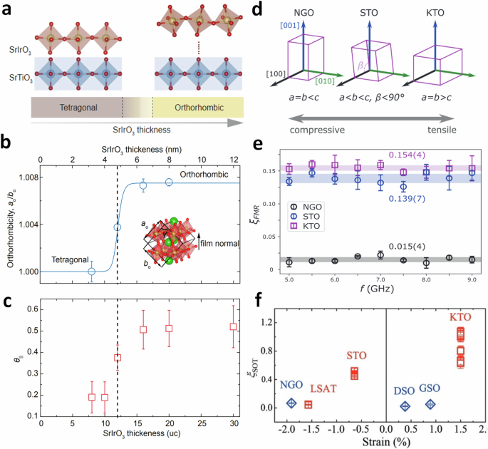
a–c SrIrO384: a Schematic of thickness dependence of octahedral rotation in SrIrO3. b Thickness dependence of orthorhombicity ao/bo. c Thickness dependence of SHA in Py/SrIrO3. d–f SrRuO3116,119: d Schematic illustration of the effects of epitaxial strain on the lattice parameters of SrRuO3116. e SOT efficiency of SrRrO3 on KTaO3(KTO), SrTiO3(STO), and NdGaO3(NGO) substrates116. f SOT efficiency of SrRrO3 on NdGaO3(NGO), (LaAlO3)0.3(Sr2TaAlO6)0.7(LSAT), SrTiO3(STO), NdGaO3(NGO), DyScO3(DSO), GdScO3(GSO), and KTaO3(KTO)119.
The influence of crystal symmetry on spin Hall conductivity σSH (SHC, defined as the product of SHA θSH and charge conductivity σc, σSH=θSH∙σc) is also evident in SrRuO3116,117,118,119. SrRuO3 film, epitaxially grown on KTaO3(KTO) substrates with large tensile strain (Fig. 2d), developed orthorhombic phase and had SHA as large as 0.154 (Fig. 2e)116, whereas compressively strained SrRuO3 thin film on NdGaO3(NGO) substrates present tetrahedral phase with a reduced SHA of ~0.015, —-an order of magnitude smaller (Fig. 2e)116. Similar trends were also confirmed by a different research group, which reported that the altering the strain from compressive to tensile via epitaxial growth could enhance the SOT efficiency of SrRuO3 thin films from 0.04 to 0.89, where the crystal structure was tuned from tetrahedral to orthorhombic (Fig. 2g). Although the trend of SHA changes in SrRuO3 due to epitaxial strain is consistent across the above mentioned two works, the measured value of the SHA vary significantly. This discrepancy could be attributed to several factors, including difference in thickness of the heterostructures, sample quality or disparities in interfacial spin transmission. It’s a commonly known that epitaxial strain in thin film would decrease with growing film thickness due to strain relaxation. This effect has been extensively studied120 and demonstrates a significant thickness dependence of spin and electronic properties in tensile-strained SrRuO3 thin films. Additionally, the type of single crystal oxide substrate used can induce different artifact signals in SOT measurements, particularly in ST-FMR experiments. These artifacts can substantially influence the interpretations of strain effects on the spin-Hall effect, highlighting the need for careful consideration of experimental conditions and substrate choice in SOT research121.
Reconfigurable strain
Under epitaxial strain, which is discrete and limited by the mismatch condition of hetero-epitaxy, reconfigurable strain allows for the application of strain in a larger scale and/or in a continuous manner122,123.This method utilizes piezoelectric substrates or flexible substrates that can be mechanically deformed by compressing, stretching or bending. Consequently, thin films grown on these substrates adapt to the deformation, resulting in dynamically adjustable strain. Recent studies have demonstrated significant enhancements of SOT in heavy metals using reconfigurable strain engineering.
For example, in a CoFeB/Pt/PMN-PT(011) hybrid structure124, as shown in Fig. 3a, piezoelectric strain has shown to not only modulate SOT efficiency (Fig. 3b), but also to induce an effective magnetic anisotropy and rotate the easy axis (Fig. 3c). This modification facilitates the in-plane magnetization switching and can significantly reduce the switching time by a factor of 3.
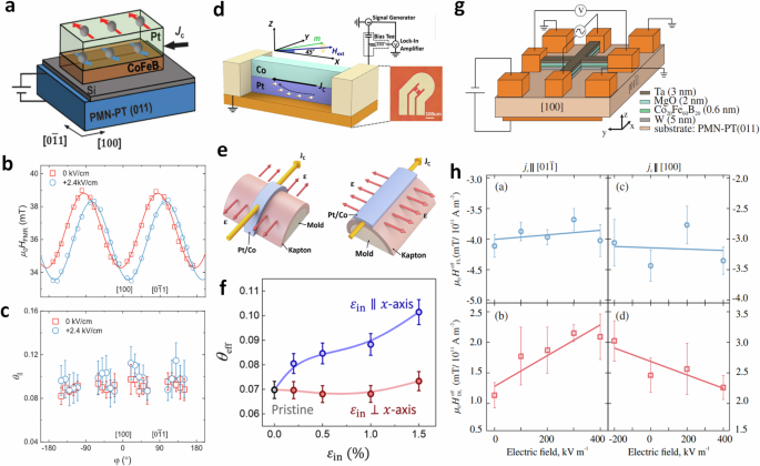
a–c Pt/piezoelectric124: a Geometry of CoFeB/Pt/PMN-PT(011) device. b Resonance field HFMR as a function of in-plane magnetic field angle for different applied electric (c) spin Hall angle of CoFeB/Pt/PMN-PT device. d–f Pt/Co bilayer system125: d Schematic illustration of a Pt/Co bilayer for the ST-FMR measurement. e Schematic of strain application onto the sample. f Spin Hall efficiency as a function of in situ tensile strain. g, h W/piezoelectric126: g Schematic of the Ta/MgO/CoFeB/W/PMN-PT(011) Hall bar (h) FL and DL SOT effective fields under compressive (left) or tensile (right) strain.
In Pt/Co bilayers, applying tensile strain along the current axis enhanced the spin Hall efficiency from 0.07 to 0.1, as shown in Fig. 3d–f125, with 78% of the enhancement retained even after removing the strain. A linear relationship was observed between tensile strain and spin Hall efficiency, attributed to increased spin-dependent collision between the conduction electrons and ions.
Further in W/CoFeB/MgO multilayers (Fig. 3g, h)126, both compressive and tensile strains modulated the anti-damping torque in W, enhancing it by a factor of 2 under 0.03% tensile strain, as shown in (Fig. 3g). First principle calculation revealed a strain-induced crystal symmetry transformation from fourfold C4v to twofold C2v, resulting in a redistribution of the d-states of the conduction electrons and leading to enhanced intrinsic spin Hall effect.
Reconfigurable strain is not limited by the constraints of hetero-epitaxy, allowing for strain modulation even in polycrystalline SOT materials. This capability has been exploited to enhance the spin Hall angle (SHA) in polycrystalline heavy metals with strong spin-orbit coupling (SOC), further demonstrating the utility of reconfigurable strain engineering in advancing SOT technologies125,126.
Interface engineering
Interface engineering represents a pivotal approach in enhancing the effective SOT efficiency in the heterostructures. Firstly, it improves spin transparency within the spin source/ferromagnet (FM) layer interfaces, crucial for efficient spin current transmission and effective manipulation of magnetization. Secondly, interface engineering serves to protect and stabilize topological surface states in the topological materials/FM heterostructure, which are essential for leveraging the unique properties of topological materials in spintronic devices.
Enhancement of spin transparency
Interface engineering plays a crucial role in improving SOT efficiency by enhancing spin transparency in heavy metal (HM)/ferromagnet (FM) heterostructures. In these heterostructures, a pure spin current, generated via SHE, transports across the interface to apply torques onto the adjacent magnetic layers. The transmittivity of this spin current transport across an interface is evaluated by the interfacial spin transparency, which includes contributions from spin backflow (SBF) ({{rm{T}}}_{mathrm{int}}^{{SBF}}) and spin memory loss (SML) ({{rm{T}}}_{mathrm{int}}^{{SML}})71,73,127,128. The SBF refers to the back diffusion of the spin current due to spin scattering at the interface, and the SML involves the flipping of spins when the spin current crosses the interface due to the interfacial spin-orbit coupling. The total spin transparency ({{rm{T}}}_{{int}}^{{SBF}}, {{rm{T}}}_{{int}}^{{SML}}) and the SML ({{rm{T}}}_{{int}}^{{SML}}) could be expressed as,
where ({G}_{{HM}/{FM}}^{downarrow uparrow }) is the bare spin-mixing conductance of the HM/FM interface71,128, ({G}_{{SML}}) is the effective spin memory loss (SML) conductance of the interface, and ({G}_{{HM}}=1/{rho }_{{xx}}{lambda }_{s}) is spin conductance of the HM, ({rho }_{{xx}}) is the resistivity of the HM and ({lambda }_{s}) is the spin diffusion length of the HM. Improving the spin transparency Tint would lead to an enhanced SOT efficiency. And engineering the HM/FM interface, such as oxidizing the interface or incerting an oxide layer to the interface, is found to effectively improve the spin transparency. For instance, increasing the oxygen concentration in the W layer of the SiO2/W(O)/CoFeB/TaN structure129, led to a substantial rise in SOT efficiency, peaking at an oxygen concentration of 12.1%. The enhancement of SOT efficiency was considered to originate from the oxygen interface regulation. In another work, the SOT efficiency of the CuOx/Py bilayers was improved by changing the oxygen concentration130, which was also attributed to the interfacial regulation of oxygen.
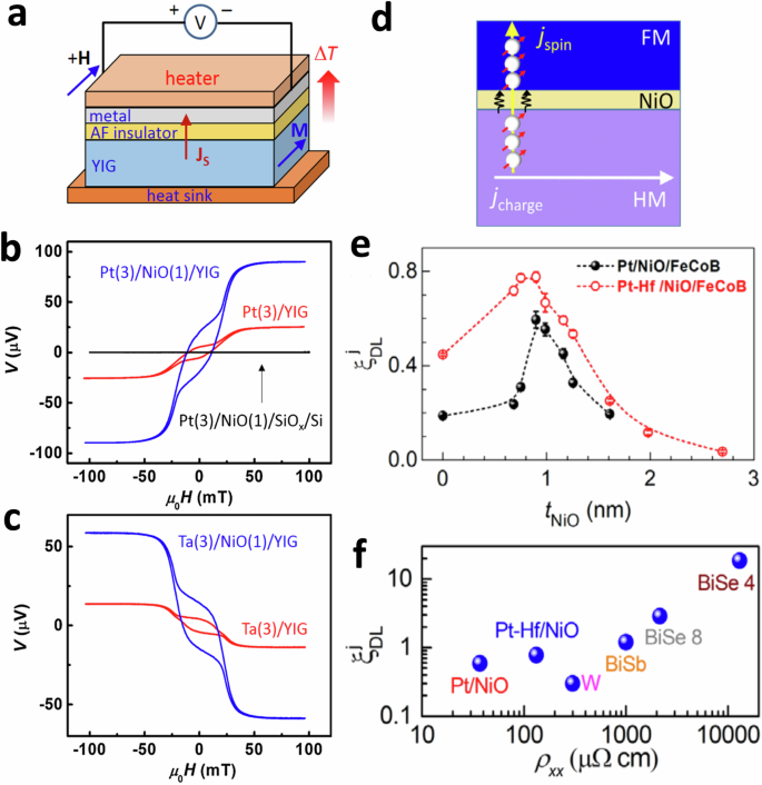
a–c Spin Seebeck experiment in HM/NiO/YIG: a Schematic diagram of the Spin Seebeck experiment for the HM/NiO/YIG structure131. b, c Inserting 1 nm of NiO into Pt/YIG and Ta/YIG structures can significantly increase the Spin Seebeck voltage131. d–f HM/NiO/CoFeB132: d Schematic of the HM/NiO/FM devices. e Spin Hall efficiency varies with NiO thickness132. f Comparison on estimated power of HM/NiO and other typical SOT materials132.
Insertion of an oxide layer into the HM/FM structure is also found to influence the SOT efficiency. For instance, incerting an antiferromagnetic NiO layer into the Pt/YIG interface increases the spin current, which is generated via spin Seebeck effec and measured via inverse spin Hall effect, up to an order of magnitude (Fig. 4a–c)131. This enhancement is attributed to the presence of the spin fluctuation in the NiO layer, which amplifies the spin current transmission, especailly at temperature that is near Néel temperature. In the Pt/NiO/FeCoB structure, the insertion of approximately 1 nm thick NiO layer markedly enhanced spin transparency (Fig. 4e–f)132. However, when the NiO layer’s thickness exceeded 1 nm, a decline in SOT efficiency was observed, likely due to the limited spin diffusion length of NiO. Contrastingly, in the Bi2Se3/NiO/NiFe, there is an enhancement of the SOT efficiency at NiO thickness of ~20 nm, which can be attributed to the presence of the magnon-mediated spin torque62.
Engineering of topological surface states
Engineering the surface states of spin source materials, especially in topological materials, is a crucial strategy for enhancing SOTs. The significant SOTs in these materials predominantly originate from the spin-momentum locking due to the presence of their surface states133. However, challenges arise in maintaining the integrity of these states when interfaced with ferromagnetic layers (FM). For instance, in the heterostructure of Bi2Se3/Ni(Co)134, the intrinsic topological surface state of Bi2Se3 was disrupted. Detailed band structure analysis using density functional theory calculation and tight binding model showed discrepancies in work functions led to the shifting of topological states below the Fermi level, merging with the metallic bands of Ni(Co) and thus degrading the spin-helical structure. This phenomenon was corroborated in studies with an elemental topological Dirac semi-metal α-Sn, where angle-resolved photoelectron spectroscopy (ARPES) indicated the destruction of topological surface states upon deposition of a thin Fe layer of 0.9 Å (Fig. 5a)135. To preserve these critical states, several strategies have been implemented. In α-Sn structures, insertion a thin layer of Ag on the α-Sn film not only protected the Dirac cone from disruption (Fig. 5a), but also enhanced spin current absorption capabilities, evidenced by significantly increased Gilbert damping (Fig. 5b)136. Further, this Ag layer insertion in an α-Sn/CoFeB structure facilitated effective magnetization switching by maintaining the topological states (Fig. 5c)86.
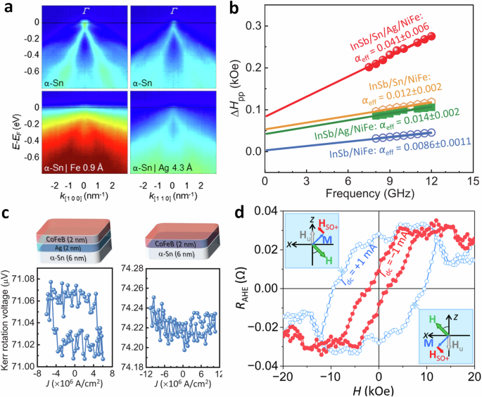
a Comparison of ARPES results among α-Sn, α-Sn/Fe, and α-Sn/Ag structures135. b Comparison of magnetic damping in different structures136. c Current-induced magnetization switching via topological surface states α-Sn protected by the insertion Ag layer86. d Loop shift in Bi2Se3/BaFe12O13 structure with different currents90.
Substituting the ferromagnetic metallic layer with a ferromagnetic insulating layer has also shown promise in preserving topological states. In Bi2Se3/BaFe12O19 structure90, where BaFe12O19 is a ferrimagnetic insulator, the topological surface states of Bi2Se3 remained intact and effectively generated polarized spin currents for magnetization switching, demonstrating high SOT efficiency (Fig. 5d).
Symmetry engineering
Perpendicular magnetization is highly valued in low-power high-density magnetic memory and logic devices, making deterministic switching of perpendicular magnets essential6,137,138. Anti-damping torque ({tau }_{{AD}},propto ,{bf{m}}times ({bf{m}}times {boldsymbol{sigma }})) generated by spin current with polarization ({boldsymbol{sigma }}) can switch magnetic moments effectively and deterministically when the easy axis aligns with the direction of the polarization ({boldsymbol{sigma }}). Consequently, a perpendicular magnet can be switched deterministically via a z-polarized anti-damping torque ({{boldsymbol{tau }}}_{{boldsymbol{AD}},{boldsymbol{z}}}). Yet, most spin source materials are found to generate spin–orbit torque corresponding to y-polarization due to symmetry restrictions. Because the spin angular momentum is an axial vector (or pseudovector), a spin current with z-polarization would change its sign under mirror reflection in xz plane ({hat{{boldsymbol{M}}}}_{{boldsymbol{y}}}:(x,y,z)to (x,-y,z)), which contradicts the translational symmetry present in the materials. This restriction prohibits the generation of z-polarized spin current (see Fig.1c)39,40. An external magnetic field along the current direction is typically required to break the symmetry and facilitate the deterministic switching, which is, however, unpractical for applications.To realize the field-free deterministic switching of perpendicular magnets, various strategies of mirror symmetry breaking have been developed and can be classified into the following three categories:
(1) Asymmetric device design: This approach involves breaking mirror symmetry by introducing asymmetric design features at the device level, such as non-uniform distribution of film thickness and composition variations.
(2) Crystalline symmetry breaking: This approach involves mirror symmetry broken due to the inherently low symmetry of the lattice structure.
(3) Magnetic symmetry breaking: This approach involves mirror symmetry breaking by the introduction of long-range magnetic ordering in the spin source layer, such as a cluster magnetic octupole moment in non-collinear antiferromagnets (AFM), a Néel vector in collinear antiferromagnets, and a magnetic moment from a FM layer.
In this section, we review recent research progress on current-induced, deterministic, field-free switching of perpendicular magnetization through symmetry engineering in spin source/FM structures.
Asymmetric device design
Asymmetric device design introduces structural asymmetry at the device level to break mirror symmetry, achievable through non-uniform distributions of film thickness39,138 and composition139,140,141,142,143.
For instance, in the Ta/CoFeB/TaOx(wedge) heterostructure39, where the TaOx layer has a wedge shape with a linearly changing thickness across the lateral direction (Fig. 6a), current-induced field-free switching of perpendicular magnets was observed. This switching was attributed to a new field-like effective field in the z-direction ({{boldsymbol{H}}}_{{boldsymbol{z}}}^{{boldsymbol{FL}}}), arising from the lateral thickness-gradient, which facilitated the switching of the perpendicular magnetization. Reversing the current direction to oppose the thickness gradient resulted in an opposite switching polarity, as shown in the current-induced switching measurements (Fig. 6b, c)39. This further demonstrated that the effective field ({{boldsymbol{H}}}_{{boldsymbol{z}}}^{{boldsymbol{FL}}}) is dependent on the thickness-gradient. A similar wedge structure in a Ta/CoFeB(wedge)/MgO multilayer also enabled field-free switching of the perpendicular magnetization (Fig. 6d)138. The trapezoidal shape of the edges in these structures breaks the symmetry and provide an intrinsic bias magnetic field, enabling field-free switching of perpendicular magnetization (Fig. 6e, f)138.
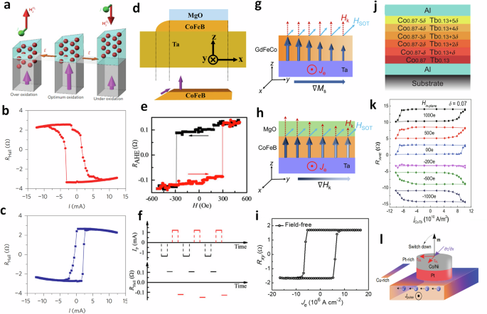
a–c Ta/CoFeB/TaOx(wedge)39: a Schematic of generating oop effective field ({{boldsymbol{H}}}_{{boldsymbol{z}}}^{{boldsymbol{FL}}}). Current-induced switching with current along one (b) and the opposition c thickness-gradient direction. d–f Ta/CoFeB(wedge)/MgO138: d Schematic of the heterostructure. e Anomalous Hall resistance. f Current-induced switching. g–i Lateral magnetic gradient142: g saturation magnetization Ms or h magnetic anisotropy field Hk. i Magnetization switching with charge current. j–k Vertical composition gradient in CoxTb1-x139: j Schematic of vertical composition distribution of the CoxTb1-x film. k Current-induced perpendicular magnetization switching. l Cu–Pt143: Schematic of Cu–Pt/Pt/Co/Ni heterostructure with lateral composition gradient in Cu–Pt layer.
In addition to lateral thickness-gradient, lateral gradient of composition in the spin source layer or magnetic layer have been also reported to break mirror symmetry and realize field-free switching of perpendicular magnetization140. The lateral composition gradient in Cu–Pt spin source layer, as depicted in Fig. 6l, generated a lateral gradient of SOT and broke mirror symmetry143. Composition gradient in magnetic layer modulated the saturation magnetization Ms (Fig. 6g) or magnetic anisotropy field Hk (Fig. 6h), generating non-collinear spin texture with in-plane components. The Dzyaloshinskii–Moriya interaction (DMI) which broke chiral symmetry, resulted in deterministic switching without an external field (Fig. 6i).
Introduction of vertical asymmetrical structures has also been reported to contribute to field-free switching of perpendicular magnetization. In a ferrimagnetic Co1-xTbx thin film with perpendicular magnetic anisotropy(PMA), where the components of Co and Tb continuously changed in the vertical direction and formed a composition gradient (Fig. 6d)139, researchers observed current-induced field-free switching of the perpendicular magnet in Co1-xTbx film. This was attributed to the presence of a composition gradient-driven DMI, which broke the xz mirror symmetry and allow generation of a z-polarized torque.
The advantages of using the asymmetric device design lies in its versatility; it can be applied to various types of spin source materials, including the simple heavy metals which are compatible semiconductor technology. However, adaptation of these designs for use in SOT-MTJ devices and scaling them up for industrial mass production still requires experimental demonstrations. These developments are crucial for validating the designs’ compatibility and feasibility in practical applications.
Crystalline symmetry breaking
Asymmetric device design represents an “extrinsic” approach for achieving symmetry breaking. In contrast, symmetry breaking arising from the inherent material structure such as crystalline structure is “intrinsic”.
Crystalline symmetry breaking can be realized in spin source materials with intrinsic low crystalline symmetry95,144,145,146. Transition-metal dichalcogenides, for example, are particular notable for their for their strong SOC and low crystalline symmetry, making them prime candidates for this approach. Significant z-polarized SOT has been observed in materials like tungsten ditelluride WTe2 which possesses a layered orthorhombic structure with the space group Pmn21144,147,148,149,150. In a WTe2/Py bilayer, an out-of-plane anti-damping torque with corresponding SOT efficiency of 0.016 and SOT conductivity of (3.6 ± 0.8) × 103 (ℏ⁄2e) Ω−1 cm−1 is reported (Fig. 7a–c)144. Besides, it is found that this unconventional torque is crystalline orientation dependent. Angle-dependent asymmetry components VA from Lorentzian fitting of ST-FMR spectra reveals the presence of an out-of-plane anti-damping torque when charge current is in a-axis direction (Fig. 7b).When current is along b-axis with mirror symmetry the out-of-plane anti-damping torque vanishes (Fig. 7c). In addition, thickness dependence study reveales a decreased trend of this z-polarized SOT with increasing WTe2 film thickness, indicating its interfacial origin in the WTe2/FM heterostructure147. Field-free switching of two-dimensional(2D) PMA magnets via the z-polarized SOT was also demonstrated in WTe2/PMA structure150. Other transition-metal dichalcogenides with similar crystalline structure as WTe2 are also found to show SOT with z polarization. In MoTe2/Py structure, a small out-of-plane anti-damping torque efficiency of 0.005 was reported, as well as the same crystalline-dependent trend151. While in NbSe2, unconventional torque was not observed, which was attributed to crystalline change under strain during device processing152 .
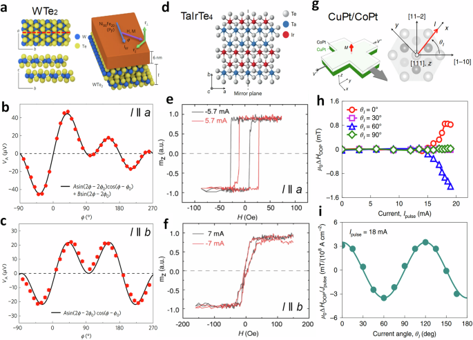
a–c WTe2/Py structure144: a Schematic of the crystalline structure(left) and device(right). Angle-dependent asymmetry components VA from ST-FMR spectra when current ran (b) along a-axis (c) along b-axis. d–f TaIrTe4/Py structure146: d Schematic of the crystalline structure. Hysteresis loop shift measurement when current ran e along a-axis (f) along b-axis. g, h CuPt/CoPt structure96: g Schematic of the device(left) and crystalline structure at the interface(right), h current-induced out-of-plane effective field from loop-shift measurement, and i crystalline orientation dependence of the out-of-plane effective field per current density.
Apart from transition-metal dichalcogenides, recent study on ternary 2D material, Weyl semimetal TaIrTe4, also reports observation of a large out-of-plane SOT with similar crystalline orientation-dependent (Fig. 7d–f)146. Loop shift measurement in the absence of an in-plane magnetic field shows shift and an out-of-plane effective field when charge current aligns with a-axis (Fig. 7d). And the shift disappears in the anomalous Hall loop when current is along b-axis where a mirror present (Fig. 7f). The SOT efficiency of this unconventional torque is estimated to be 0.043 ± 0.003 from ST-FMR measurement, with SHC of (2.065 ± 0.014) × 104 (ℏ⁄2e) Ω−1 cm−1, which is around 1/3 of its conventional y-polarized SOT efficiency. The same trend of the out-of-plane anti-damping torque on the TaIrTe4 thickness is also found.
In addition to 2D materials/FM bilayers, investigation on heterostructures based on CoPt have led to several interesting findings.
In the L11-ordered CuPt/CoPt heterostructure96, the low crystallilne symmetry at the interface leads to generation of an unconventional SOT with maximum effective field of 0.03 mT per 106 A/cm2 (Fig. 7g–i). Loop shfit measurements reveals that an out-of-plane effective field µ0ΔHOOP exists when charge current is at the low crystalline symemtry direction, for instance, when the current angle θI is 0° or 60° (Fig. 7h). The presence of the threhold current indicats an out-of-plane anti-damping torque. More detailed experiments shows this out-of-plane effective field has a threefold rotation symmetry with respect to the current angle (Fig. 7i). The corrsponding torque is denoted as “3m” torque due to the symmetry. Similar result is also reported in single magnetic layer, an A1-disordered Co30Pt70 alloy thin film, where the same trend of the SOT effecitve field on current direction is observed95. In this case, the presence of the SOT and the free-field switching of the same layer is attributed to the cooperation of two structural mechanisms: the low crystal symmetry at the Co platelets/Pt interfaces which gave rise to the “3 m” torque, and the composition gradient along the thickness direction which broke the mirror symmetry along the z-plane. However, in another study a field-like torque corresponding to the x-polarization instead of z-polariztion is reported in a [Pt/Co]5/CoFeB multilayer, where the Co films is ultrathin (t < 0.260 nm) and presents paramagnetic state153. In this structure, symmetry breaking is considered to be obtained through a weak in-plane magnetization of Co, acquired from the stray field of the adjacent in-plane magnetized CoFeB film via magnetic proximity effect.
In brief, out-of-plane SOTs can be generated from a spin source layer with low crystalline symmetry and with mirror symemmtry breaking. The magnitude of the out-of-plane SOTs hence depend strongly on the crystalline orientation.
Magnetic symmetry breaking
Magnetic ordering in magnetic SOT materials offers an alternative “intrinsic” approach to break mirror symmetry. The presence of long-range magnetic ordering has been proven to effectively break mirror symmetry and lead to generation of unconventional SOTs. For instance, investigation on non-collinear AFM materials reports the presence of unconventional SOT due to the presence of chiral spin texture in real space and its resulting band splitting in k-space, which is denoted as the magnetic spin Hall effect (MSHE)82,100,154,155,156. These non-collinear AFM materials include Mn3GaN, Mn3SnN, Mn3Sn, Mn3Ga, MnPd3, and so on.
Mn3GaN is a metallic manganese nitride of anti-perovskite crystalline structure, and belongs to the space group ({rm{Pm}}bar{3}{rm{m}}). The spins of the Mn atoms form Kagome structure in the (111) plane due to magnetic frustration, reducing the mirror planes to only one in (110) (Fig. 8a)157,158. Unconventional torques corresponding to z-polarization and x-polarization were reported by ST-FMR measurement (Fig. 8b)154. Temperature dependent ST-FMR study shows that these unconventional torque vanish when the sample temperature is larger than the Néel temperature of Mn3GaN, confirming the important role of the magnetic structure in generating unconventional torques. Out-of-plane SOT also is also found in Mn3SnN thin film with the similar crystalline and magnetic structure (Fig. 8c)156, and field-free switching of perpendicular magnetization is also demonstrated (Fig. 8d).
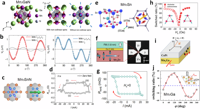
a, b Mn3GaN structure154: a Anti-perovskite crystalline structure and the non-collinear spins(left), the (001) projection with (middle) and without (right) non-collinear spins. b Symmetry and asymmetry component from ST-FMR spectra indicating the presence of unconventional SOTs when current run along [100] direction. c, d Mn3SnN structure156: c spin texture(left) and the cluster magnetic octupole moment T. d field-free switching of PMA via an out-of-plane torque. e–h Mn3Sn structure100: e Crystalline structure(left) and the cluster magnetic octupole moment T(right) along the (0001) direction. f Schematic of the device. g Field-free switching of PMA via z-polarized torques and h switching polar(clockwise or anticlockwise) reversed with changing spin texture. i, j Mn3Ga structure145: i Schematic of the device and j crystalline orientation-dependent switching ratio on the (0001) plane.
Mn3Sn is hexagonal structure belonging to the P63/mmc space group and a non-collinear AFM with Kagome plane on the (0001) plane (Fig. 8e). Out-of-plane and conventional anti-damping torques were reported in the Mn3Sn/Cu/FM structure (Fig. 8f)100. In loopshift measurement where charge current was in the Kagome plane and aligns with the cluster magnetic octupole moment T, the corresponding SHA of out-of-plane torque and conventional torque were evaluted to be 0.067 and 0.22, respectively. Field-free switching in the Mn3Sn/Cu/PMA structure showed efficiency switching at 20 mA with critical current density of 5×10⁶ A/cm2 (Fig. 8g). The switching polarity(clockwise or anticlockwise) and switching ratio is not symemtric with respect to the magnetic fields due to a preferred AFM domain orientation in Mn3Sn during the deposition process (Fig. 8h). And in the field-free switching experiment in the Mn3Ga(0001)/PtCo heterostructure145, the switching polarity and switching ratio present a sinusoidal relation with respect to the current direction (Fig. 8i, j). It is also worth mentioned that when the non-collinear AFM works as a detected layer instead of a spin source layer, the octupole moment in the Mn3Sn layer rotates in an opposite direction with the individual moments under SOT switching, resulting in a distinct SOT switching polarity from ferromagnets159.
A summary of electric resistivity, SHA of the out-of-plane torque θz, SHA of the conventional torque θy, the ratio θz/θy of spin source materials with intrinsic symmetry breaking is listed in Table 1.
The generation of an in-plane component of magnetization or effective magnetic field is another way for magnetic symmetry breaking. In PtMn/CoNi structure, where Néel vector of the AFM film PtMn is lying in-plane, investigation showed that deterministic switching of the perpendicular magnetization in CoNi via current-induced spin–orbit torque was realized without the aid of an external magnetic field (Fig. 9a–c)160. Because the spins in ferromagnetic CoNi layer near the interface were pinned at the Néel vector direction due to exchange coupling, an in-plane exchange field appeared and broke the mirror symmetry, allowing generation of out-of-plane SOTs. In other AFM/FM systems, such field-free switching of perpendicular magnets were also demonstrated, such as in the IrMn/CoFeB161, PtMn/CoFeB162 stack structures.
A tilted magnetic moment is also an effective approach to offer in-plane symmetry breaking. In an epitaxial grown Pt/Co heterostructure, dislocations generates crystal lattice tilting with respect to the substrate plane, leading to a tilted magnetic easy axis deviated from the perpendicular direction (Fig. 9d)98. The in-plane component of this tilted magnetic moment breaks the mirror symmetry (Fig. 9e). And field-free switching of the tilted magnetic moment in Pt/Co heterostructure was also demonstrated (Fig. 9f). Tilted magnetic anisotropy axis and field-free switching is also achieved in ferrimagnetic Gd/Co multilayers163. In an epitaxial collinear antiferromagnetic ruthenium dioxide RuO2(101) film, where the Néel vector in [001] direction was tilted relative the sample plane, an out-of-plane anti-damping torque was also found via ST-FMR measurement164.
An in-plane magnetic moment from an extra magnetic layer could also help to break mirror symmetry. In epitaxial-Co/HM/FM trilayers (Fig. 9g)165, it is reported that the large in-plane magnetocrystalline anisotropy(IMA) in epitaxial Co film ensures a magnetic moment component in the current direction (mepi-Co || x) (Fig. 9h), which breaks the mirror symmetry and leads to field-free switching of perpendicular magnetization (Fig. 9i).
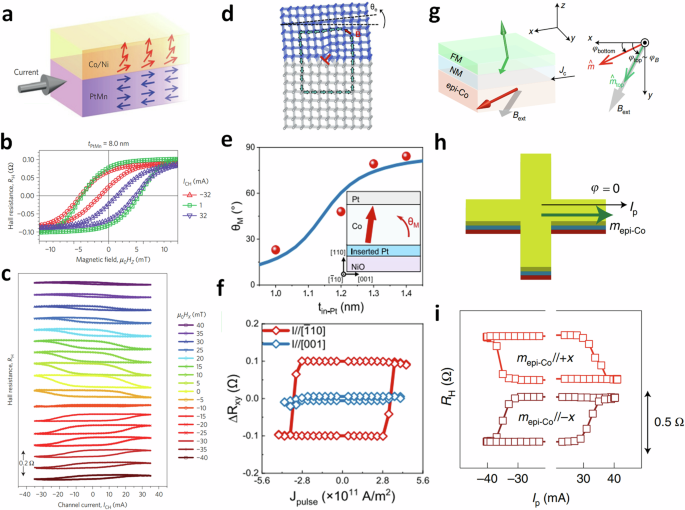
Mirror symmetry breaking via (a–c) AFM-FM exchange field in PtMn/CoNi structure160: a Schematic of the spin orientation, b Hall resistance showing the presence of an exchange field, and c current-induced magnetization switching. d–f Tilted magnetic moment in Pt/Co/Pt/NiO structure98: d Schematic of the dislocation leading to tilted crystalline planes. e The tilted magnetic moment varied with the thickness of insertion Pt layer and f current-induced magnetization switching. g–i In-plane magnetic moment with strong IMA in Co(epi)/NM/FM structure165: g Schematic of the trilayer. h Schematic of the Hall bar measurement setup with magnetic moment of Co(epi) lying in the current direction and i current-induced field-free magnetization switching.
Summary and outlooks
Optimizing spin source materials through material design is a promising pathway toward power-efficient spintronic application. This includes strain engineering, interface engineering and symmetry engineering. Strain engineering has led to enhanced SOT efficiency in complex oxides, heavy metals and alloys. Interface engineering led to protected topological surface states and improved spin transparency. Symmetry engineering enabled deterministic, field-free switching of perpendicular magnets via symmetry breaking approaches, such as asymmetric device design, crystalline symmetry breaking and magnetic symmetry breaking.
Despite these advancements, significant challenges remain in fully harnessing the potential of SOTs through material design: (1) Strain Engineering: A comprehensive understanding of how crystalline structure influences electronic properties and spin-Hall conductivity, especially in complex oxides, is still lacking. This is important for the design of artificial materials optimized for maximized spin-orbit torque (SOT) efficiency. Addressing this gap requires a multidisciplinary approach involving theoretical studies, advanced materials characterization techniques, and artifact-free spin torque measurements. Furthermore, the development of new experimental methods capable of applying larger and more tunable strains to single-crystalline SOT materials is crucial. Innovations such as free-standing single crystalline films on flexible substrates could enable more profound modulation of the strain effects on SOT, leading to significant enhancements in SOT efficiency. (2) Interface Engineering: The mechanisms by which the insertion of antiferromagnetic oxide layers at interfaces enhances spin transparency remain ambiguous, particularly regarding the potential roles of magnon-mediated currents, which is still a subject of active debate. Despite these uncertainties, integrating antiferromagnetic or multiferroic materials at the interface provides substantial benefits. These materials introduce additional functionalities and enable voltage tunability in spin-orbitronic devices, offering new ways to manipulate spin currents and magnetic states effectively. (3) Symmetry Engineering: The precision required in asymmetric device design and the handling of materials with low crystalline symmetry or long-range magnetic ordering pose significant challenges, particularly in terms of scalability and manufacturing consistency. Addressing these issues is crucial for the transition from laboratory settings to industrial-scale production.
In conclusion, while the field of spintronics has seen considerable progress due to innovative material engineering strategies, ongoing research is essential to address the remaining technical challenges. Future work will need to focus on refining these engineering approaches and developing new methodologies to fully realize the potential of spin-orbitronics devices for next-generation beyond-CMOS technologies.


Responses