Revolutionizing wearable technology: advanced fabrication techniques for body-conformable electronics

Introduction
The evolution of electronic devices, driven by the emergence of semiconductors and integrated circuits, has transformed them from bulky and cumbersome to compact and increasingly powerful1,2. The rapid development of the Internet of Things (IoT) and artificial intelligence (AI) has led to the innovations of new morphological electronic devices tailored for practical applications, such as mechanical flexibility, particularly in advanced medical and healthcare monitoring technologies. The demand for seamless integration of flexible and wearable devices with the human body, regardless of force-induced deformation during body movements, has created a pressing need for body-conformable electronics. Traditional rigid electronics are unable to meet the market demand for physical and functional properties of devices, making the transition from rigid to flexible/stretchable electronics an inevitable outcome of technological progress and market demands3,4.
Since the 21st century, flexible and stretchable electronics have experienced remarkable development and gained widespread attention from both academia and industrial communities5,6. These new morphological electronics have revolutionized the design and functionality of electronic products, surpassing the limitations of rigid and fragile substrates7. They can be bent, folded, and even stretched, and their performance does not degrade or only experiences minor loss during the deformation process, thereby greatly expanding their range of applications8,9. Among various application fields, flexible and stretchable electronic devices have particularly excelled in the domain of wearable devices. Flexible and stretchable electronic devices with features such as design freedom10, lightweight portability11, seamless integration12, and multifunctionality13, which have played a significant role in advancing wearable technology development14,15,16,17, including human-machine interfaces (HMI)18,19 and healthcare monitoring20,21. Furthermore, with the continuous development of IoT8,22,23,24 and AI technologies25,26, flexible and stretchable electronics are poised to play an increasingly crucial role in emerging fields of wearable electronics.
As technology advances, wearable electronic devices are becoming smarter and more efficient in HMI and medical health monitoring27,28,29. They not only provide real-time monitoring and feedback but also offer personalized advice and treatment plans to users through data analysis, thereby improving the quality of life and health status30. For example, health monitoring bracelets utilize flexible electronics technology to achieve real-time monitoring of the user’s health status31, and smart textiles integrate flexible sensors to monitor the wearer’s physiological parameters32. The design of bio-integrated electronics and the application of biocompatible materials have reduced irritation to human tissues, making them more suitable for long-term wear or implantation33,34,35,36,37,38. Additionally, flexible electronics technology holds great potential for future IoT sensor networks, enabling smaller, more flexible sensors that can be deployed in various environments on the human body39,40. These advancements have not only enhanced the user experience but also brought revolutionary changes to the healthcare industry.
Significant advancements have been made in the field of flexible electronics fabrication technology. This includes progress in the fabrication of flexible display arrays, flexible sensors, and stretchable batteries, which provide a better experience for body-comfort electronic systems compared to traditional rigid electronic systems38,41,42. Flexible display technology provides users with innovative interaction methods and new visual experiences43. Flexible sensors find wide applications in health monitoring and environmental sensing due to their thin, lightweight, and bendable characteristics44,45. The development of flexible battery technology offers wearable devices more durable power support46. Advances in conductive ink and printed electronics technology have enabled more flexible and lower-cost fabrication of electronic devices47. Body-conforming electronics, compared to traditional electronics, can better adhere to the skin surface and maintain good contact during movement. This helps to improve the signal-to-noise ratio and accuracy of the human body signals collected27,48,49. Chen and others developed flexible Au/PU electrodes for testing myoelectric signals, achieving a signal-to-noise ratio as high as 21.29 dB and an accuracy rate of 92.4%, which is significantly higher than the traditional metal electrodes’ 12.06 dB signal-to-noise ratio and 83.1% accuracy rate48. In addition, the flexibility of the devices allows them to adapt well to the morphological changes at different parts of the human body, which greatly improves their long-term clinical application35,50. For example, Yang and others developed a 3D structured flexible device that achieved a record of neuro-organ physiological electrical signal recording for up to 120 days50. However, to better meet the needs of applications, the fabrication technology of flexible electronics still faces many challenges that need to be addressed.
To address the challenges in the fabrication process, such as integrating high-performance electronic components on flexible substrates, achieving high-precision and high-resolution patterning, and ensuring stable device performance under external deformation51,52,53,54, various advanced manufacturing technologies have been developed. These include screen printing, spray coating, roll-to-roll (R2R) technology, soft transfer, soft lithography, 3D printing, fiber/fabric technology, kirigami technology, and mechanical guided assembly technology. These technologies excel in surface treatment, precise transfer of micron- and nanometer-scale devices, direct fabrication of 3D structures, and deformation fabrication of flexible electronics, providing a solid technological foundation for the development of wearable electronics. They have made significant strides in the development of flexible and stretchable electronic products, thoroughly meeting the demand for lightweight, deformable, and stable electronic/photonic devices. The continuous breakthroughs in flexible electronics fabrication technology have propelled the advancement of wearable electronics from enhancing the quality of life to driving medical innovation, and further promoting sustainable development.
In this review, we focus on the specific applications of flexible electronics fabrication technology in wearable/body-conformable electronics, delving into key processes such as printed electronics fabrication, soft transfer, 3D structure fabrication, and deformation fabrication, as shown in Fig. 1. Additionally, it provides a summary the current state of development of flexible electronics fabrication/manufacturing processes, anticipates potential future technological breakthroughs, and offers an outlook for continued research and technological innovations in wearable electronics.

printed electronics fabrication technology, transfer technology for flexible electronics85,146,147, 3D structure fabrication technology, and deformation fabrication technology. The technologies mentioned encompass several other branches. Spray coating148,149, screen printing64,150,151, and roll-to-roll152,153 belong to the category of printed electronics fabrication technology. Fiber/fabric technology154,155, 3D printing156,157, and soft lithography158,159 are part of 3D structure fabrication technology. Mechanically guided self-assembly technology141,160 and kirigami techniques129,161 fall under the category of deformation fabrication technology.
Printed electronics fabrication technology
Printed electronics fabrication technology is an additive fabrication method that employs a printing or coating process to create electronic components, circuits, and systems on flexible or bendable substrates. This technology encompasses various techniques such as screen printing, spray coating, and R2R processes. Screen printing involves the deposition of conductive or semiconductor materials onto a substrate through a screen, enabling the formation of circuits or electronic components. Spray coating utilizes a spray gun to uniformly spray electronic materials onto a substrate, making it suitable for manufacturing large-area or shape-specific electronic components. R2R is a continuous production line process that allows materials to be processed on a roll, enabling large-scale production through operations like coating, printing, and cutting. These technologies share commonalities in flexible electronics manufacturing, enabling the realization of a wide range of designs and functionalities such as conductivity, functionality, and protection by precisely controlling the type, thickness, distribution, and pattern of the deposited materials. However, they differ in specific applications such as accuracy, resolution, thickness control, production scale, and manufacturing speed. Each technique has its advantages and considerations depending on the desired outcome and production requirements.
Printed electronics fabrication technology has evolved from traditional manufacturing processes, gradually finding its niche in wearable electronics through advancements in achieving higher precision and reliability. Efforts focused on flexible sensors and energy harvesting devices have harnessed the potential of printed electronics, where the creation of conductive patterns on flexible substrates is paramount for circuitry in wearable devices. Consequently, the primary thrust of furthering printed electronics lies in the development of novel inks and substrates that are more flexible, durable, and conductive.
Integrating printed electronics fabrication technology with other advanced fabrication techniques, such as 3D printing, promises to yield highly precise multi-layered structures, enabling the creation of wearable electronic devices with enhanced functionalities. As production scales up to a significant level, the inherent sustainability of printed electronics fabrication technology will translate into substantial cost benefits for the wearable device industry.
Spray coating
Spray coating is primarily utilized for depositing conductive materials or functional coatings, such as those aimed at enhancing water-resistance55 or mechanical properties56. Commonly employed conductive materials for spray coating include Ag nanowires (AgNWs)57, carbon nanotubes (CNTs)55, graphene, and MXene58. These materials are appropriately diluted and can be effectively used in spray coating processes. The fundamental principle of spray coating involves atomizing a liquid or powdered material using compressed air or an inert gas such as nitrogen or helium, and uniformly spraying it onto a flexible substrate. To achieve patterning in spray coating, a stencil corresponding to the desired pattern is designed and produced. The stencil ensures that only specific areas receive the spray material, thereby creating the intended pattern. Patterned spray processes can be employed to create conductive paths56, sensor patterns59, and display devices60. By precisely controlling the spraying parameters and stencil designs, high-precision and resolution in patterning can be achieved, reaching up to the microscale level56.
In the field of flexible electronics manufacturing, spray coating is particularly suitable for applications that require large areas and rapid deposition of coatings, including the fabrication of flexible solar cells61, flexible displays62, and flexible circuit boards63. Fig. 2a illustrates a schematic of the spraying technique. Su et al. utilized spray coating to deposit the active layer in an 8 × 8 display array, improving the layer’s uniformity60. Photographs of the flexible organic light emitting diode (OLED) display array in bent states are shown in Fig. 2b, c. The successful application of spray coating in flexible OLEDs has demonstrated its potential for wearable electronics, which can be applied to the monitoring of human physiological parameters, such as photoplethysmography (PPG). However, it is important to note that spray coating technology also has some limitations to address, such as the potential generation of harmful gases and dust during the spraying process. Additionally, ensuring the uniformity of the coated layers remains an important challenge.

a The schematic diagram of spray coating. b, c is an array of flexible OLED displays fabricated by spray coating technology. The display is bent inward (b) and the graph displayed when the display is bent inward (c)60. d The schematic diagram of screen printing64. e Photograph of fully screen-printed electrodes when twisted64. f Photographs of metal-polymer electrode array patches during bending and twisting66. g The schematic diagram of roll-to-roll (R2R) printing. h SEM image of the R2R-printed double re-entrant microstructures with a diameter of about 30 μm75. i Photograph of flexible perovskite solar cell fabricated by R2R gravure printing76.
Screen printing
Screen printing is a printing technique that utilizes a tautly attached screen frame as a stencil, allowing ink with functional materials to be squeezed through the screen openings onto the substrate using a squeegee. Functional materials include conductive64, luminescent65, and heat-sensitive66 materials, while substrates such as polyethylene naphthalate (PEN)67, polyimide (PI)64, and polyethylene terephthalate (PET)66 are commonly used. Similar to spray coating, screen printing finds applications in flexible solar cells68, flexible displays65, and flexible circuit boards69. Fig. 2d provides a schematic diagram of screen printing, where a customized patterned screen plays a crucial role in mold formation, and the mesh count of the screen determines the printing precision. Precise control over the direction of squeegee movement and pressure is necessary to ensure high-quality prints. Current screen printing conditions allow for achieving accuracy at the microscale level65.
Recent advancements in screen printing have contributed to the development of flexible and wearable electronics. Park et al. presented the screen-printed electrodes for electrocardiograph (ECG) monitoring64. These skin-attached electrodes were entirely manufactured using screen printing, exhibiting excellent mechanical properties and sensing properties. An optical image of the electrode during twisting is presented in Fig. 2e. Yang et al. developed a metal-polymer electrode array patch, as depicted in Fig. 2f, which consisted of a liquid metal circuit and poly(3,4-ethylenedioxythiophene) poly(styrenesulfonate) (PEDOT:PSS) electrodes fabricated through screen printing. This fully stretchable structure enabled motion monitoring66. However, screen printing does have certain limitations. The need for frequent replacement of screen templates can significantly impact production speed.
Roll-to-roll (R2R)
R2R technology is a continuous printing method that involves depositing functional materials such as perovskite, graphene, conductive inks, and LEDs onto a substrate while it is transferred from one roll to another70,71,72. This technology utilizes various printing techniques such as offset printing, gravure printing, screen printing, nanoimprinting, or inkjet printing to continuously apply ink patterns onto substrates like paper71 and plastic films70,71 at a high speed. Fig. 2g shows a schematic diagram of R2R production, which includes mounting a large roll of the substrate onto a reel, printing functional materials onto the substrate, and drying it for further processing. R2R finds extensive applications in flexible electronics, including flexible solar cells, flexible antennas, flexible batteries, and flexible displays73, thanks to its advantages of high speed, high volume, and automation advantages70,71,74.
The growing demand for large-area micro- and nano-patterned surfaces with functionality in various emerging applications of flexible electronics has led to the exploration of R2R fabrication. Large-scale production of surfaces with micro- and nanostructures has been achieved using flexible molds in R2R processes. However, limited mold reproducibility has hindered its commercialization. To address this issue, Kim et al. implemented an ultraviolet (UV)-curing-based R2R system to replicate polyurethane acrylates (PUAs) microstructures, enabling large-scale printing of micro- and nanostructures with improved mold reproducibility. The number of mold cycles increased from 10 to over 1000 cycles75. Fig. 2h displays a scanning electron microscopy (SEM) image of a double re-entrant pore microstructure printed using a UV-curing-based R2R system. The high throughput advantages of R2R technology offer significant potential for the commercialization of flexible electronics. Bisconti et al. achieved high-volume production of flexible perovskite solar cells using the R2R gravure printing process (shown in Fig. 2i), opening up possibilities for perovskite solar cells to enter the market76. However, R2R technology has certain drawbacks, including strict substrate requirements, the need for precise tension control, and limitations in printing shaped objects.
Soft transfer technology
Soft transfer technology is a crucial technique for achieving the transfer of wearable electronic devices from a donor substrate to a receiver substrate. The essence of soft transfer technology revolves around controlling the adhesion and peeling force of the materials involved. By carefully managing the peel speed, contact area, and interface temperature, a stamp is able to pick up and release devices during the transfer process. Soft transfer technology is applicable to various materials, such as micro-sized metal particles, two-dimensional materials, silver films, graphene films, carbon nanotube network films, and quantum dots (QDs), thereby facilitating the widespread adoption and utilization of wearable electronics77. Soft transfer technology has been effectively utilized in the field of body-comfort electronics for health monitoring in bio-integrated electronics35. For instance, ultrasonic ceramic patches are transferred onto flexible substrates to create ultrasonic imaging arrays for monitoring heart rate and blood flow velocity78, and μ-LED are transferred onto flexible substrates to phototherapy79. These applications showcase the potential of soft transfer technology in wearable electronics for health monitoring.
Concurrently, soft transfer technology confronts a multitude of challenges, including the imperative to ensure high transfer efficiency and yield rates, compatibility issues when accommodating diverse material properties, and the maintenance of device performance and stability in real-world applications. With ongoing technological innovation and refinement, soft transfer technology is poised to realize further breakthroughs and applications within the wearable electronic device sector. Anticipating the ongoing evolution of wearable electronic devices, soft transfer technology is projected to enhance its precision and reliability, adapt to various environmental conditions, and achieve scalability in production.
Thermal release transfer
Thermal release transfer typically involves the use of thermal release tape or the interaction force between the stamp and the device79 to pick up the device. By heating the stamp, the adhesion strength between the device and the stamp is reduced, allowing for the release of the device. Yang et al. realized the pickup of MoS2 by the van der Waals force and subsequently realized the release of the device by heating the stamp80. Fig. 3a is a schematic diagram of the large-scale transfer of MoS2 arrays by the thermal release transfer. Fig. 3b is a schematic diagram of the circuit array formed after realizing the precise release of the device. The greatest advantage of this method lies in its basis on a simple heating process, which is easy to operate and implement, but the issue of potential thermal damage during the release process cannot be overlooked.

a Schematic diagram of the large-scale transfer of MoS2 arrays by the thermal release transfer technology80. b Schematic diagram of the circuit array formed the thermal release transfer technology80. c Schematic of the process of adjusting the contact area between the stamp interface and the device with a laser to release the material83. d Optical images of different patterned objects transferred by Laser-driven non-contact transfer technology83. Scale bar: 200 μm. e Schematic diagram of the working principle of the bioinspired adhesive structure with controllable weak and strong adhesion modes84. f SEM image of resin plates which transferred by bioinspired adhesive structure84. Scale bar: 20 μm. g Schematic diagram of picking up and transferring a micro-nano device onto a receiving substrate by using a shape memory polymer (SMP)162. h Transferring micro-LEDs with SMP, the micro-LEDs remain illuminated after the transfer162. i Schematic representation of the surface chemistry and adhesion transfer technique, and finally the release of the device by utilizing the etching of the sacrificial layer85. j Capacitors transferred to the tape85.
Laser-driven non-contact transfer
Laser-driven non-contact transfer employs laser pulses to heat the interface between the stamp and the device, thereby modulating the temperature and delaminating the device from the stamp, which is then released onto the receiving substrate. One approach relies on high temperatures generated by the laser to reduce the adhesive force between the device and the stamp81, similar to thermal release transfer. The other approach utilizes the laser’s high temperature to expand the gas inside the stamp, reducing the contact area between the stamp and the device, and facilitating the release onto the receiving substrate82. Fig. 3c illustrates the process of modulating the contact area between the stamp and the device interface using a laser to achieve material release83. Under UV light, the stamp expands as a whole, reducing the contact area, while infrared radiation (IR) light further promotes the expansion of small microspheres on the stamp’s surface to further reduce the contact area, thus achieving the purpose of releasing the material. This method enables the transfer of microchips smaller than 100 μm, as shown in Fig. 3d. Laser-driven non-contact transfer offers high selectivity and flexibility for operating on specific areas. However, laser parameter adjustment can be complex, and there is a risk of thermal damage to devices.
Shear-assisted transfer
Shear-assisted transfer employs shear to regulate the adhesion strength between the stamp and the device, enabling device transfer. This technique relies on the differences in adhesion strength between the pickup and release directions. Pang et al. proposed a mushroom-shaped biomimetic adhesive structure that utilizes shear for the pickup and release of the devices84. Fig. 3e illustrates the working principle of the bionic adsorption structure with controllable weak and strong adhesion modes. As shown in Fig. 3f, this structure allows for the transfer of 100 μm-sized devices. Shear-assisted transfer minimizes damage to 2D materials during the transfer process. However, precise control of the magnitude and direction of the shear force remains a challenging aspect for further research.
Shape memory polymer transfer
Shape memory polymer (SMP) transfer utilizes the properties of SMP to pick up and release devices by changing their shape. When stimulated, the SMP recovers its original shape, facilitating the release of the embedded object. Linghu et al. proposed a universal transfer method by utilizing SMP to pick up and release devices. This method enables the transfer of devices as small as 10 μm. Fig. 3h demonstrates the schematic of an LED chip transferred to a polydimethylsiloxane (PDMS) substrate using this approach. SMPs allow for flexible control during the transfer process and improve transfer accuracy by returning to their initial shape upon appropriate stimulation. However, SMPs may experience fatigue over repeated deformation and recovery processes, which can affect their long-term stability and reliability. Additionally, some SMPs exhibit longer response times, which may impact transfer efficiency.
Surface chemical and adhesive transfer
Surface chemical and adhesive transfer uses the adhesion of an intermediate polymer layer for device transfer and release. Glue or chemical treatments are usually used to enhance the adhesion during the pickup process, and chemical reactions are used to reduce the adhesion or etch the sacrificial layer during the release process for device transfer. Liu et al. utilized the sacrificial layer approach to assist nanotransfer, and large-area nanoscale patterns (such as 100 nm-thick, 4 mm-long, and 47 nm-wide arrays of gold nanowires)85 were achieved. Fig. 3i shows the transfer process of the surface chemistry and adhesion transfer technique. A sacrificial layer is deposited on the donor and the device is constructed on this layer. The device is subsequently transferred to the receiving substrate along with the sacrificial layer, and the transfer process is completed by etching the sacrificial layer. Fig. 3j shows the eight capacitor devices transferred to tape by means of the technique. It is particularly suitable for the transfer of large-area thin films or devices, but the impact of residues left after the transfer on the transferred devices remains a non-negligible issue.
3D structure fabrication technology
Wearable electronic devices typically require complex 3D structures to fulfill their specific functions. While planar manufacturing technologies have been working to fulfill this need, they have limitations in creating complex 3D structures. 3D structure fabrication technologies, including soft lithography, 3D printing, and fabric technologies, are able to create these complex geometries directly and accurately. Wearable electronic devices normally require the integration of multiple functions, such as sensing, display, energy storage, etc.86,87. 3D structure fabrication techniques allow for the integration of these functions on the same platform, improving the integration and performance of the device.
Soft lithography technology
Soft lithography is a micro- and nanoscale 3D structure fabrication technology that utilizes flexible materials (e.g., polymers or elastomers) as stamps to form micron- or nanoscale patterns on a substrate through physical contact or chemical interaction in a direct or indirect manner87,88. Based on the basic concept, various soft lithography techniques have been developed, including contact transfer-based microcontact printing (μCP), contact transfer microtransfer molding (μTM), solvent-assisted capillary micromolding (SAMIM), and capillary micromolding techniques (MIMIC) that rely on capillary forces. These techniques are widely used for fabricating 3D structures. Soft lithography offers significant advantages for flexible electronics fabrication. It provides cost benefits, particularly in low-volume or lab-scale applications. Moreover, soft lithography allows the fabrication of complex and high-resolution microstructures on non-planar substrates and is relatively simple to execute. The realization of high-resolution patterning at low cost is crucial for the further development of body-comfort electronics. These technologies find extensive applications in microfluidic chips, biosensors, nanoelectronic devices, and optical components89. However, there are certain challenges associated with soft lithography that need to be addressed. The low accuracy of alignment, which relies on manual operation, is an area that requires improvement. Additionally, accurately stacking multiple layers in the fabrication of multilayer structures remains a challenge that needs to be overcome in this technology. Soft lithography technology has unveiled significant potential and prospective applications within the micro- and nano-manufacturing domain. In biomedical applications, the deployment of flexible biosensors and microfluidic devices is anticipated to catalyze the evolution of personalized healthcare and the proliferation of point-of-care diagnostic methodologies.
Microcontact printing (μCP)
μCP, the most mature soft lithography process, is a method used for patterning molecular ink onto a surface with an elastic stamp. In this process, the desired molecules such as metals and nanoparticles are applied to the stamp, which is then brought into conformal contact with the substrate. When the stamp is removed, the molecular ink pattern is left on the substrate (Fig. 4a)90,91. This method offers several distinct advantages that exhibit the superior capability to achieve high-resolution patterning of molecular films with resolutions as fine as sub-micron levels92. In some cases, stamps have been mounted on microscopes or motorized systems, enabling higher precision, repeatability, and higher throughput. Yalcintas et al. developed a high-precision automated μCP system that facilitates both the loading of the stamps and the application of liquid metal (LM), such as eutectic gallium-indium (EGaIn) patterns, onto the substrate. By using this method, circuits with line widths as small as 15 µm were successfully fabricated, without encountering short-circuit issues caused by printing residues93. The optical image of a micro-resistor printed onto a finger is shown in Fig. 4b. Overall, μCP demonstrates its efficacy in achieving precise and high-resolution patterns, especially when combined with advanced automation techniques. This method proves particularly useful in fabricating micro-resistors and other intricate structures on various surfaces.

a General scheme for microcontact printing (μCP). b Optical photograph of a micro-resistor printed onto a finger by using μCP93. c General scheme for microtransfer molding (μTM). d SEM image of quantum dots (QDs) with 350 nm resolution printed by μTM technology87. e General scheme for capillary microforming (MIMIC). f Optical photograph of a hexagon structure on PDMS fabricated by MIMIC technology88. g General scheme for solvent-assisted micromolding in capillaries (SAMIN). h SEM images of MXene nanopatterns with a height of 600 nm and a width of 2 µm fabricated by using SAMIM technology95. Scale bar: 5 μm.
Microtransfer molding (μTM)
μTM is a soft lithography technique that builds upon μCP and enables the transfer of 3D structures in a single step, unlike μCP, which is limited to transferring molecular layer inks. In this method, a liquid prepolymer is applied to an elastomer stamp and brought into contact with the substrate. The molded prepolymer takes on the desired shape and is then cured through methods such as irradiation, heating, or the use of a gelling agent. Once the polymer is cured, the elastomer stamp is peeled off, leaving behind the desired microstructure on the substrate (Fig. 4c). One limitation of soft lithography is the potential deformation of the stamp due to elastomer properties. To address this issue, PDMS stamps can be replaced with rigid stamps made of materials like polymethyl methacrylate (PMMA). Nam et al. used PMMA stamps instead of the conventional PDMS stamps to achieve the alignment and printing of individual RGB pixel arrays with printed QDs printed at nanometer-scale sizes87. They achieved a resolution of 350 nm in the printed quantum dot array, as shown in the SEM image of Fig. 4d. By utilizing μTM, researchers can overcome the limitations of molecular ink transfer and realize the fabrication of complex 3D structures in a single step. The use of rigid stamps, such as PMMA, further enhances the accuracy and resolution of the printed patterns, enabling the precise alignment and printing of nanoscale features, as demonstrated in the case of printed QD arrays.
Capillary microforming (MIMIC)
The MIMIC technology integrates μTP and microfluidics to fabricate micron- or nanoscale 3D microstructures on a substrate using capillary forces. This technique is particularly well-suited for creating microstructures on hard materials such as silicon, glass, or other inorganic materials88,94. The fabrication process of MIMIC is illustrated in Fig. 4e. An elastomer mold with a micro-channel array is in contact with the substrate and injected with a polymer liquid. Capillary action ensures that the liquid fills the channels, and once the polymer cures, the PDMS mold is removed, revealing the cured microstructure.
MIMIC has been successfully employed for patterning high-resolution polymers, and it has demonstrated the ability to print materials such as metallic nanowires. However, its capability has been limited to simple patterns on rigid planar substrates. To address this, Liu et al. conducted a study using MIMIC to print AgNWs on flexible substrates, achieving excellent resolution down to 20 μm and outstanding mechanical properties88. Moreover, the printed patterns can be printed on cylinders, hemispheres, and even arbitrary curved surfaces. An optical photograph of a hexagonal structure printed onto PDMS is shown in Fig. 4f. Despite significant progress, several challenges remain for MIMIC technology. These include improving the durability and repeatability of the mold, enhancing precision during the liquid filling process, and addressing the potential requirement for high temperatures in certain applications. Overcoming these challenges would further enhance the reliability and applicability of MIMIC for advanced microstructure fabrication.
Solvent-assisted micromolding in capillaries (SAMIM)
SAMIM technology utilizes solvents to facilitate the molding of microstructures. The principle behind SAMIM involves temporarily swelling the elastomer stamp with a solvent, which promotes the complete filling of channels. As the solvent evaporates and the stamp shrinks, the polymer becomes effectively trapped within the microstructure. The process flow of SAMIM is depicted in Fig. 4g. The stamp is brought into conformal contact with the substrate by placing a droplet of liquid polymer or prepolymers onto the substrate, allowing the liquid to fill the stamp. Once the liquid fills the stamp and the polymer or prepolymer cures, the mold is removed, resulting in the formation of the desired 3D microstructure.
SAMIM exhibits several advantages over standard MIMIC, including enhanced adaptability to highly viscous polymers and improved filling ability for stamp microstructures. Song et al. demonstrated the fabrication of vertically aligned MXene using a PDMS stamp, achieving line widths of less than 200 nm and a microstructure height of about 600 nm (Fig. 4h)95. However, SAMIM still faces certain challenges. The choice of solvent must consider their solubility with the elastic stamp and the substrate material, as well as their potential environment and health impacts on operators. Additionally, achieving the right balance between solvent evaporation rate and capillary forces is crucial for accurately replicating the desired microstructures.
3D printing technology
3D printing, an additive manufacturing technology, builds objects layer by layer under computer control. The efficiency of depositing each layer determines the printing speed. There are two primary types of 3D printing techniques based on the material deposition method: photopolymerization and extrusion96. Within the photopolymerization methods, stereolithography (SLA) and digital light processing (DLP) are widely used processes that utilize light to cure a stack of photosensitive inks. In the extrusion method, fused deposition modeling (FDM) and direct ink writing (DIW) are commonly employed techniques that create 3D structures by re-solidifying extruded materials in continuous layers.
3D printing technology holds immense potential in the field of flexible electronics fabrication due to its advantages of high design flexibility, material savings, and elimination of assembly processes. However, it is still an emerging technology in flexible electronics and requires further refinement and advancement. Key areas for improvement include enhancing production scale and precision, as well as expanding the range of materials suitable for wearable electronics applications. 3D printing technology applies to a wide range of materials, and with the deepening of material technology research, more and more new materials have been put into use, including self-healing materials. Body-comfort electronics may suffer from friction, bending, stretching, and other mechanical damages during daily use. Self-healing materials can automatically repair after the material is damaged, extending the service life of electronic devices38,97. Self-healing materials made from 3D-printed hydrogels or hydrogel composites have been widely used in biomedicine and electronic devices98,99. 3D printing technology provides an efficient, flexible, and precise molding method for hydrogel self-healing materials, which helps to promote the application of such smart materials in body-conforming electronics100. The maturation of 3D printing technology will contribute to its wider adoption and successful integration into the wearable electronics industry.
Photopolymerization method—stereolithography (SLA) and digital light processing (DLP)
SLA and DLP are both light-curing 3D printing technologies that construct 3D structures layer by layer using a specific wavelength of light source (UV or laser) to cure liquid photosensitive resins. The standout feature of SLA and DLP among 3D printing technologies is their exceptional resolution. The distinction between them lies in the curing of the single-layer pattern; SLA employs a single spot of light to traverse a flat surface and cure the resin, creating a 2D pattern, while DLP projects the entire 2D pattern to cure the resin101. In the field of flexible electronics, SLA and DLP are used to fabricate devices with intricate geometries and precise microstructures.
SLA, one of the earliest light-curing 3D printing techniques, involves a laser moving through a pool of resin along a computer-controlled path to selectively cure the resin to build up layers and form a 3D model (Fig. 5a). SLA is renowned for its high resolution and ability to capture intricate details, reaching resolutions of up to hundreds of nanometers96. An et al. demonstrated the fine detailing capability of SLA by printing flexible cubes with porous structures102, as shown in Fig. 5b. SLA technology has advanced in the integration and application of flexible sensors. Fig. 5c shows an SLA-printed artificial fingerprint sleeve, capable of capturing touch-sensing signals103. However, SLA printing is relatively slow and necessitates the use of expensive lasers.

a The schematic diagrams of stereolithography (SLA). b A flexible cube printed by SLA102. c An artificial fingerprint-like sleeve printed by SLA103. d The schematic diagrams of digital light processing (DLP). e Photograph of a firefly-shaped device printed with DLP technology104. f A hydrogel cardiovascular scaffold with drug release capabilities printed with DLP technology105. g The schematic diagrams of fused deposition modeling (FDM). h Printed twisted vases with a wall thickness of 0.8 mm which allow reversible deformation109. i Schematic of an antenna worn on the human body, with the serpentine wire molded and encapsulated in FDM-printed thermoplastic polyurethane110. j The schematic diagrams of direct ink writing (DIW). k Continuous printing of ink through a 75 μm needle112. l Photograph of a liquid metal coil affixed to the wrist that is integrated with radio frequency identification (RFID)113. m The schematic diagrams of s omnidirectional printing (ODP). n Images of elastic wiring made from the emulsion-based elastic conductive ink with a series of self-supporting 3D geometries117. o Image of high-resolution printing (~50 µm) of the PILC ink118.
DLP is an evolved version of SLA that employs digital micromirror devices (DMDs) to control the light source distribution. During DLP printing, a digital projector projects an image of the entire layer, which is cured by an array of micromirrors on the DMD, selectively illuminating the liquid resin (Fig. 5d). The highly customizable nature of DLP technology is exemplified by the firefly-shaped device printed in Fig. 5e. DLP has broad application scenarios in multifunctional flexible devices, particularly in biomedical devices104. Ge et al. utilized a self-built DLP-based multimaterial 3D printer to print hydrogel-polymer blends, showcasing a physical image of a hydrogel cardiovascular scaffold with drug-releasing functionality in Fig. 5f105. The ability of DLP to cure an entire layer in one go significantly improves printing speed and enables the construction of larger volumes. However, compared to SLA, DLP has a lower resolution, reaching up to a few tens of micrometers.
Extrusion method—fused deposition modeling (FDM), direct ink writing (DIW), and omnidirectional printing (ODP)
FDM involves the melting of thermoplastic polymers into filaments through a heated nozzle, which is then stacked and fused layer by layer to construct 3D structures (Fig. 5g). Commonly used thermoplastic materials in FDM include polycarbonate (PC) polylactic acid (PLA), acrylonitrile butadiene styrene (ABS), and polyurethane (PU)106. The properties of the printed material can be enhanced by incorporating additives such as carbon fibers or carbon nanotubes during the printing process107,108. FDM is particularly suitable for large-scale printing, allowing the preparation of structures on a meter scale. A significant advantage of FDM is its capability for multi-nozzle printing, enabling the simultaneous or staged printing of materials with different properties to achieve customization. Heiden et al. introduced a customized 3D printing method based on FDM, showcasing its potential for structural design and sensor integration in soft robotics109. Fig. 5h shows an optical photograph of a printed twisted vase with a wall thickness of 0.8 mm, showcasing its soft structure and low Young’s modulus, enabling reversible deformation. FDM also plays a crucial role in the design and fabrication of flexible human health monitoring devices. Fig. 5i presents a schematic of an antenna worn on the human body for transmitting sensor signals, with a serpentine metal wire shaped and encapsulated using FDM-printed thermoplastic urethanes (TPU)110. However, the limitation of FDM lies in its ability to print only thermoplastic materials, which has hindered its further advancement. The print resolution is influenced by the nozzle size, with the highest accuracy being approximately 100 μm.
DIW is a 3D printing technology that employs a computer-controlled syringe or nozzle to precisely extrude a specially formulated viscous ink material, which is deposited and solidified onto a substrate to form a 3D structure (Fig. 5j). DIW exhibits greater versatility in material selection, allowing the printing of hydrogels, ceramics, polymers, composites, and other materials using this technique106. Moreover, DIW enables the mixing of multiple materials for printing111. Chen et al. further improved the printing accuracy of DIW by utilizing specially prepared ink, achieving a printing accuracy of 70 μm112. Fig. 5k illustrates the continuous printing of ink through a 75 μm needle. Yamagishi et al. developed a DIW-based microfluidic electronics method that utilizes the injection of liquid metal into 3D-printed microchannels to fabricate flexible and stretchable liquid metal coils. Fig. 5l displays a photograph of the liquid metal coil integrated with radio frequency identification (RFID) attached to a human wrist113. DIW faces the challenge of using ultra-high viscosity materials for direct writing, and the impact of ink rheology and processing parameters on resolution and shape is still not fully understood114.
Omnidirectional printing (ODP) involves the extrusion of inks or materials with special rheological properties that are self-supporting during the printing process, enabling the print head to print in the air or on a non-planar substrate, thus realizing complex 3D structures (Fig. 5m). ODP is capable of being applied to a wide range of materials, including conductive materials, emulsion elastomer composites, and biomaterials115,116. ODP is an innovative 3D printing technology with significant benefits. The use of self-supporting inks during the printing process can significantly reduce or even eliminate the need for support structures. The high degree of freedom of multi-directional printing allows for the printing of finer and more complex structures, as well as a significant increase in print speed, which is particularly beneficial for mass production and rapid prototyping. Despite the advantages of omnidirectional printing, there are challenges such as precise control of the print head, planning of the multi-directional print path, and material selection and compatibility. For body-comfort electronics, there are still challenges in realizing ODP for stretchable electronics. Lee et al. reported the ODP of electronics using an emulsion-based elastomeric conductive ink to achieve the ODP of stretchable electronics (Fig. 5n)117. The ink consists of an emulsified elastomer composite with immiscible non-volatile solvents and silver particles and multi-walled carbon nanotubes that provide sufficient stability to self-support the printed 3D structure, allowing direct printing of electrodes to create freestanding out-of-plane 3D geometries with more than 150% strain and dimensions with less than 100 μm resolution. Byungkook Oh et al. reported a 3D printable PEDOT:PSS-ionic liquid colloidal (PILC) ink (Fig. 5o)118. PILC can be rapidly prototyped, supports vertical stacking with high aspect ratios, is suitable for generating suspended structures, and prints with a resolution of up to 50 μm, which can be applied in the fields of flexible circuit boards and electronic skin. These efforts advance the development of ODP technology in the field of body-comfort electronics.
Fiber/fabric technology
Fiber/fabric technology in the field of manufacturing technology for 3D structures mainly refers to electrostatic spinning, thermal drawing, and coating. Electrospinning and thermal drawing can directly produce functional fibers119,120. Coatings impart new functionalities to fibers121,122. Smart clothes constitute a captivating arena within the domain of wearable electronic technology, with capabilities to monitor health metrics, deliver haptic responses, and regulate temperature. The application of fiber/fabric technology facilitates the integration of electronic components, sensors, and conductive interconnects into the fabric substrates of smart clothes, laying the groundwork for the advancement of wearable technology in this sector123.
The envisioned culmination of smart clothes innovation is a wearable product that embodies intelligence, comfort, durability, and eco-sustainability. The fiber/fabric technology, while endowing fibers with functionality, must also consider the demand for wear and age resistance of the fibers. Concurrently, the innovation of novel eco-friendly materials stands as a pivotal aspect within the research and development agenda of this field.
Thermal drawing
Thermal drawing is a direct fiber forming technique that involves extruding polymers in a molten state from a nozzle inside a drawing furnace, followed by cooling (Fig. 6a). The resulting fibers typically have diameters in the range of several hundred microns and offer numerous advantages, including high mechanical strength, stable electrical properties, and precise internal structure. Thermal drawing enables continuous and large-scale fiber production and finds extensive applications in polymer formation. For instance, Zhou et al. achieved the production of kilometers of MXene fibers using fluid-assisted thermal drawing, wherein PC-coated MXene fibers exhibited high electrical conductivity and high mechanical properties119. The schematic representation of the PC-coated MXene fiber structure is depicted in Fig. 6b, while Fig. 6c displays a SEM image of the twisted MXene fiber fabricated through thermal drawing. There have been useful attempts to integrate semiconductors or electronic components into a single fiber by thermal stretching to build new smart fibers. Wang et al. reported a thermally stretchable method to integrate semiconductor wires into fibers and used such fibers for wearable electronic devices to monitor the heart124. Loke et al. fabricated fibers containing hundreds of digital temperature sensors and storage devices by thermal stretching and integrated them into shirts to collect and store the wearer’s body temperature data for more accurate real-time human activity inference through AI training125. Thermal drawing has also enabled the successful integration of digital devices into fibers, resulting in fibers with digital system functionality. However, thermal drawing necessitates precise control over multiple variables, including drawing speed, temperature, and time. Additionally, careful consideration must be given to the impact of temperature on the drawn material, further adding complexity to the process.
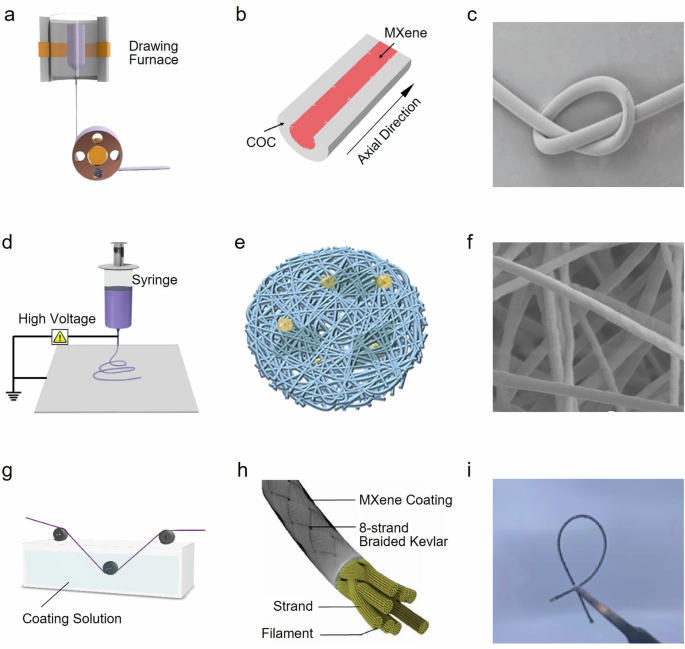
a The schematic diagram of thermal drawing. b Schematic of the MXene fiber with outer cyclic olefin copolymer (COC) layer and inner MXene nanosheets119. c SEM image of the twisted MXene fiber fabricated by thermal drawing119. d The schematic diagram of electrospinning. e Schematic diagram of nanofiber membrane fabricated by electrospinning. f SEM image of PVDF nanofiber membrane fabricated by electrospinning120. g The schematic diagram of coating. h Schematic of MXene-coated Kevlar braid fiber127. i Photograph of a twisted MXene-coated fiber127.
Electrospinning
Electrospinning utilizes an electric field to extract a solution from a syringe, which subsequently evaporates to form fibers. This technique enables the production of nanometer-scale fibers, and the addition of functional materials to the solution allows for the customization of fiber properties. The key components of electrospinning include a high-voltage source, a collection roller, and a syringe. Fig. 6d presents a schematic diagram of a basic electrospinning device. Electrospun fabrics typically exhibit a nonwoven-like structure, with fibers randomly dispersed or partially oriented to form fiber mats comprising numerous microscopic voids in single or multiple layers. A schematic structure of an electrospinning nanofiber sheet120 is depicted in Fig. 6e, while Fig. 6f shows an SEM image of an electrospun PVDF nanofiber sheet120. The surface roughness of electrospun fabrics can be adjusted by altering the type of spinning polymer or the spinning conditions. Additionally, electrospun fabrics can be integrated with various functional materials, including conductive materials, drugs, and bioactive molecules, for specific applications such as smart sensing or drug delivery. Wang et al. used electrospinning to fabricate wrinkled SMP fibers, which offer significant potential for smart controlled-release drugs and broaden the biomedical applications of electrospinning. However, electrospinning also faces certain challenges that are currently difficult to overcome. For instance, some electrospinning systems require the use of highly toxic solvents, which are expensive and not easily recyclable.
Coating
Coating is a technology that involves applying functional coating materials to the surface of fibers, imparting them with new functionalities. It offers a high level of flexibility and can be applied to various shapes and substrates. Coating techniques can generally be categorized into two types. One is to immerse the whole piece of fiber/fabric into a coating solution, resulting in the formation of a functional coating on the fabric surface. This approach has been widely used in the field of flexible fabric sensing and has been applied to the field of human health monitoring, and the application of AI can improve the accuracy of human monitoring121,126. The other is to immerse the fiber core into the coating solution and to pull it up at a constant speed. Upon the evaporation of the solution, a solid coating is formed, providing the fiber with new functionalities127 (Fig. 6g). Bi et al. developed a versatile automated coating method for the continuous production of high-quality MXene-coated yarns127. Through optimizing the coating parameters, they successfully obtained over 1 km of woven Kevlar yarn with uniform MXene coverage. The schematic diagram of the braided Kevlar yarn after MXene coating is illustrated in Fig. 6h. Importantly, the mechanical properties of the fiber remained excellent even after MXene coating (Fig. 6i). However, the development of coating techniques is hindered by durability issues, as insufficient adhesion between the coating and the substrate can lead to coating failure.
Deformation fabrication technology
Deformation fabrication technology enables precise and programmable control over material shape and configuration, resulting in significant reductions in fabrication costs and enabling personalized designs128. Leveraging this advantage, kirigami technology and mechanically guided assembly technology offer new solutions for flexible electronics manufacturing. Kirigami technology, as a static deformation fabrication technique, allows for the realization of complex 3D structures through precise cutting and folding designs, which is particularly beneficial for producing thin, lightweight, and bendable electronic devices129. This technology facilitates mass production at a lower cost while maintaining product consistency and quality. Conversely, mechanically guided assembly technology provides enhanced flexibility and accuracy. It enables real-time adjustments to components during the assembly process to accommodate different design requirements130,131,132. Although this increases system complexity, it unlocks the potential for more advanced functionality and greater customization. Both technologies possess distinct characteristics and can be employed individually or in combination, depending on the application requirements, to advance the development of highly customized and cost-effective flexible electronics.
Static deformation fabrication technology – kirigami technology
Kirigami technology leverages cutting and folding techniques to transform non-expandable sheet materials into malleable, 3D-shaped, and functional electronic devices. This process draws on inspiration from the traditional art of paper-cutting, modernized for materials, applications, and requirements of flexible electronics manufacturing. Kirigami heavily relies on flexure-induced deformation, rotational cell mechanisms, and the synergistic effects of cutting and folding129. The fabrication process mainly involves mapping complex 3D structures onto a 2D plane, precise machining of the substrate, and transforming planar wearable electronic devices into electronic devices with 3D shapes.
Benefiting from flexible design, low cost, rapid prototyping, and personalizability, kirigami technology finds widespread use in healthcare133, flexible circuits134, and smart sensing135. Particularly, it enables highly personalized production, allowing customization of the shape, size, and functions of electronic devices to meet user-specific needs. This customization capability plays a vital role in addressing the diverse market demands. Notably, user-customized features manifest in high stretchability and adaptability, tunable surface topographies, and programmable shape morphing structures. Kirigami holds great promise for innovations and offers advantages in flexible electronics fabrication. However, there are challenges to consider, including design complexities, material durability limitations, and scale-up production requirements.
High stretchability and adaptability
Unlike traditional wearable electronic devices that primarily rely on the inherent flexibility of the materials to achieve high stretchability and adaptability, kirigami technology employs a fractal-cutting strategy, which enables the creation of deformable structures such as lattices, spirals, and corrugations through cut-outs. These deformable structures, through flexure-induced deformation, rotational cell mechanisms, or synergy of both, exhibit localized folds or rotations when stretched or integrated with complex surfaces. This disperses and relieves stresses and contributes to maintaining the integrity and functionality of the cutout.
By combining flexible materials with kirigami technology, elongation limits far beyond those of kirigami structures alone can be achieved. For instance, Choi et al. introduced liquid metal-based elastic kirigami electrodes (LM-eKE) capable of stretching up to 820%136. Fig. 7a presents photographs of the LM-eKE structure at 20% and 60% strain, along with theoretically predicted deformation and von Mises color map results derived from finite element analysis. The LM-eKE electrodes offer high stretchability while maintaining shape adaptability, making them suitable for wearable health monitoring devices. Kirigami-designed electrodes with stretchable structures and shape adaptability have been utilized in implantable sensing devices, and some research teams have successfully applied these electrodes to evaluate electroencephalograph (EEG) and heartbeat signals in mice. Hong et al. applied the kirigami technology to design a structure that can achieve a stable mechanical response under deformations with tensile ratios up to 200%137. This structure was employed for vehicle tire bulge detection and human posture detection, opening a new possibility for mechanically functional materials in the field of large deformation active sensing. Fig. 7b shows photographs of the kirigami structure realizing displacement angles of 0°, 30°, 45°, and 60°, respectively, under maximum deformation conditions, demonstrating its exceptional tensile and adaptive properties.

a Photographs of experimental samples of the kirigami process at 20% and 60% strains, as well as the results of color plots of theoretically predicted deformations and von Mises stresses obtained from finite element analysis of the corresponding deformation mechanisms136. b The kirigami-designed devices were coupled to predefined displacement angles of 0°, 30°, 45° and 60° under large deformation conditions137. c Fabrication of the drug-releasable kirigami-based stents138. d Reverse design of two plants with bi-layer layouts139.
Tunable surface topographies
Tunable surface shape involves utilizing localized elastic instability to transition a surface’s topography from planar to a 3D structure, predominantly relying on the deformation mechanism of buckling. The macroscopic morphology of a material’s surface significantly influences properties such as optical characteristics, friction, and adhesion. Similarly, tunable surface topography entails employing localized elastic instability to achieve a change in surface topography from planar to a 3D structure, with the deformation mechanism of buckling playing a vital role. The kirigami technology enables the design of biomimetic structures that address real-world challenges. Inspired by scaled organisms, Babaee et al. utilized kirigami techniques to create tunable surface topography on materials138. They designed structures for shoe soles to reduce the risk of slipping and developed a drug-releasable structure. The drug-releasable stent (Fig. 7c), featuring periodic arrays of dentate needles, exemplifies the potential of kirigami technology in biomedical applications.
Programmable shape morphing structures
Programmable shape morphing structures involve the assembly of predefined 3D structures from 2D configurations, achieved through a combination of cutting and folding. This method relies on an inverse design algorithm that unfolds a given 3D surface into non-overlapping 2D patterns. They are subsequently precisely cut and assembled into 3D structures using adhesive or mechanical force. The development of an effective inverse design algorithm is a crucial aspect of designing kirigami-based programmable shape morphing structures, and it remains a challenge. To tackle this challenge, Cheng et al. have developed an analytical model and a machine learning-based algorithm for the inverse design of target 3D surfaces139. Unlike traditional inverse design methods, this algorithm programs curvature through the cutting boundaries. They have successfully utilized this algorithm to design over thirty shapes, including biomimetic 3D structures inspired by animals and plants. Fig. 7d shows the double-layer layouts obtained through inverse engineering from two types of plant flowers.
Dynamic deformation fabrication technology – mechanically guided assembly technology
Mechanical metamaterials have the potential to program mechanical strains or deformations and can be rationally designed with their microstructures to achieve materials with special mechanical properties. They are able to achieve programmable behavior through interactions between the material and the structure, thus integrating advanced functionality into their texture beyond their mechanical properties. Mechanically guided assembly technology uses the structural features of mechanically guided metamaterials to direct the assembly process of the material, enabling the automated construction of complex structures. This can be achieved through pre-programmed mechanical deformation patterns in which localized regions of the material can be controlled by external stimuli such as force, heat, magnetic or electric fields140.
Mechanically guided assembly technology leverages the mechanical properties of materials and structures to transform 2D planar devices, fabricated by well-established technologies, into 3D geometric structures. This approach caters to the requirements of wearable electronic devices that necessitate 3D structures in specific fields. This technology stands out due to its integrated design, combining device structure and function through mechanical induction. Additionally, the assembled device retains its re-deformation capability even after molding, which allows for high flexibility and accuracy by enabling real-time adjustments to components during the assembly process. The fundamental deformation modes employed to convert a 2D structure into a 3D structure encompass rolling, folding, bending, and flexing128. In this section, we will delve into commonly used mechanisms for guiding mechanical deformation, such as stress control and external stimuli control. The applications of wearable electronic devices fabricated using these techniques span a wide range, including flexible sensors130, soft robotics10, flexible circuit141, and other fields142.
Stress-controlled mechanical deformation
Stress-controlled mechanical deformation involves the creation of patterned 2D structures on a pre-stretched flexible substrate after modeling. In this process, the patterned 2D structures selectively bond with the substrate at anchor points while leaving other points suspended. Upon releasing the pre-strain, the anchor points compress the suspended points, resulting in the formation of a 3D structure driven by the substrate’s action143. The ability to mechanically guide the assembly of 3D structures is directly influenced by factors such as the selective bonding of the patterned 2D structures to the substrate, the mechanical properties of the 2D structures, and the pre-strain capability of the flexible substrate assembly platform.
The stress-controlled mechanical deformation approach is highly adaptable and suitable for various materials that can be used to create 2D structures on a plane, along with their combinations. The choice of substrate is also diverse. Several schemes have been reported for assembling 3D structures from 2D patterns on both planar and non-planar elastic substrates. Ahn et al. reported a 3D structure assembly technology suitable for nanoscale devices based on pre-stretched planar elastomers, as shown in Fig. 8a144. Xue et al. proposed a method for assembling 3D structures guided by curved surfaces. They deformed the curved elastomer into a planar structure and, after releasing the stress from uniaxial or biaxial pre-stretching, assembled the 3D structure under the action of buckling forces141. Fig. 8b illustrates the schematic of assembling a 3D piezoresistive sensor using the inner surface of a curved cylindrical tube. The tube was cut and flattened, pre-stretched about 15% in the X and Y axis directions, and then assembled in an orderly manner after removing the pre-stretch. Applications such as tunable dipole antennas, flow sensors, and electronic systems that can be conformally integrated with the heart were successfully demonstrated.

a Details of a nanoscale 3D fabrication method based on pre-stretched substrates144. b Schematic diagram of the assembly process of a 3D piezoresistive flow sensor on the inner surface of a cylindrical tube141. c Schematic of 3D structures fabricated by self-assembly based on soft electrothermal actuators131. d Flower-like structures fabricated by soft electrothermal actuators131. Scale bar: 1 cm. e Schematic diagram of reversible self-assembled 3D structure by temperature regulation145. f Photograph of reversible shape transformation by temperature regulation145. g Schematic of 3D structures fabricated by self-assembly based on light-driven soft actuators130. Flower-like structure (h) and windmill-like structure (i) fabricated by light-driven soft actuators130. Scale bar: 0.5 cm (h) and (i).
External stimuli triggered mechanical deformation
Although electricity and magnetism can also guide mechanical metamaterials toward the construction of complex structures, heat, and light are still more commonly used to trigger mechanical deformation using external stimuli. Temperature-triggered mechanical deformation is employed with thermally responsive materials, such as thermosensitive coatings and thermo-responsive shape memory polymers, which undergo deformation when exposed to heat, facilitating the assembly of 3D structures. This process involves designing a template based on the desired 3D structure, depositing thermally responsive materials at specified positions on the template, and assembling the structure through heating. Precise control of the material’s thermal response is crucial for achieving the desired assembly structure.
The ongoing development in mechanically guided 3D assembly technology focuses on designing devices with reversible shape reconfiguration capabilities to meet performance requirements. Ling et al. introduced a soft electrothermal actuator induced by laser-scribed graphene, capable of reconstructing 3D structures when subjected to heat stimulation131. Fig. 8c illustrates the fabrication process for creating 3D structures using this method. Fig. 8d presents a schematic diagram of a flower-shaped 3D structure assembled by the soft electrothermal actuator made of laser-induced graphene, emphasizing its reversible shape-changing capabilities. Zhang et al. demonstrated temperature-responsive hydrogel-driven 3D structure assembly by selectively bonding a hydrogel to a 2D membrane material, with the hydrogel controlling the formation of the 3D structure145. Fig. 8e depicts schematic diagrams of 3D structure assembly guided by temperature-responsive hydrogels, where high temperatures stimulate the hydrogel to shrink and assemble into a 3D structure, while low temperatures cause the hydrogel to unfold into a 2D plane. Fig. 8f displays optical photographs of the expanded 2D structure upon cold/hot stimulation and the self-assembled 3D structure, respectively.
The process of light-triggered mechanical deformation shares similarities with temperature-triggered mechanical deformation. However, in light-triggered deformation, light-responsive materials are employed, which deform or move under the influence of light to achieve the assembly. The key advantage of light-triggered mechanical deformation is that it can be actuated over long distances and without contact. Zhao et al. combined laser-scribed molybdenum dioxide with soft actuators to demonstrate the application of light-triggered soft actuators in reconfigurable 3D structures130. Fig. 8g presents a schematic diagram illustrating the principle of the light-triggered actuator, wherein the soft actuator undergoes deformation when driven by light. It showcased the assembled flower-like structures (Fig. 8h) and pinwheel-like structures (Fig. 8i) using this method.
Summary and outlook
The rapid advancement of flexible electronics fabrication technology, particularly its application in the wearable electronics sector, has demonstrated its immense potential and significance. This paper provides a comprehensive overview of significant progress in flexible electronics fabrication technology, including surface deposition material fabrication, soft transfer, 3D structure fabrication, and deformation fabrication. These advancements encompass material selection, processing, device assembly, and function realization. Table 1 summarizes and compares the differences in accuracy, applications, efficiency, durability, and cost between traditional and advanced electronics manufacturing technologies, highlighting their capability to meet diverse application requirements. Moreover, these technologies can be combined to achieve multilayer, multifunctional, and multidimensional fabrication of wearable electronic devices, enhancing their ergonomic compatibility and playing a pivotal role in shaping new wearable electronic devices. Fig. 9 illustrates key milestones in the development of flexible electronic devices, showcasing their evolution towards enhanced softness and shape adaptability, culminating in the realization of wearable applications. These technologies not only enhance the performance of flexible electronics and expand the scale of manufacturing but also facilitate the exploration and development of innovative designs and applications for new smart devices.

Roadmap of advanced fabrication technologies in flexible and stretchable electronics2,12,144,163,164,165,166,167,168,169,170,171,172,173,174,175,176. As advanced fabrication technology progresses, flexible electronic devices are becoming softer and more shape-adaptive, while achieving higher fabrication scales and precision, and offering a greater variety of functionalities.
Fabricating technologies for surface-deposited materials, such as screen printing, spray coating, and R2R processes, enable the deposition of functional materials onto flexible substrates to form flexible electronic active layers. These technologies offer advantages such as low cost, large area, and batch size; however, they are limited in resolution. Soft transfer technology involves transferring fabricated devices or structures to other substrates, enabling high-resolution and high-performance device transfer. Challenges related to alignment accuracy and device integrity remain to be addressed. 3D structure fabrication technology, employing methods like 3D printing, soft lithography, and fabric technology, enables the fabrication of wearable electronic devices or structures with 3D shapes, enhancing device functionality. However, this technology faces challenges such as material compatibility in 3D printing, transfer and alignment of 3D structures in soft lithography, and reliability in fabric technology. Deformation fabrication technology refers to techniques that allow materials to change shape during the manufacturing process, including the kirigami process and mechanically guided assembly. The main challenge here is achieving high-precision control during shape deformation.
Despite the remarkable progress in flexible electronics fabrication technology within the wearable electronics domain, a series of challenges must still be addressed to meet the growing market demand and diverse application scenarios. On one hand, as application requirements intensify, higher device fabrication accuracy becomes essential, which is a key determinant of wearable electronic device performance. On the other hand, the flexible electronics fabrication processes often face inefficiency and scalability issues. Many of the technologies mentioned in this paper have demonstrated their scalability advantages. Screen printing and coating technologies are adaptable to the needs of large-area electronics manufacturing and are compatible with R2R, which is considered to be the most competitive technology for mass production of flexible electronics and is highly scalable. Soft lithography and fiber/fabric technologies are also highly scalable, with the former capable of producing micro- and nanoscale patterns on a large scale, and the latter being phased into mass production. Soft transfer and 3D printing are both highly scalable and at this stage of development are more suited to customization and low-volume production. kirigami and mechanically guided assembly technologies are also scalable, creating a higher degree of freedom for flexible 3D structures, but there are still real-world challenges to be solved in the mass production process. Hence, enhancing fabrication accuracy, efficiency, and mass production capabilities remains a priority in the field. In the transition to mass production, these technologies face issues of material consistency, process integration, quality control, cost control, and environmental stability.
The development of new fabrication technologies, the improvement of established fabrication tools, the development and use of high-performance materials, and the formation of new fabrication routes are effective ways of overcoming the above problems. This will further unleash the potential and opportunities of flexible manufacturing technology, especially its application in the field of wearable/body-comfort electronics. Emerging technologies such as nanoimprint lithography (NIL), electrohydrodynamic inkjet printing, self-healing materials, stretchable conductors, hybrid printing technology, advanced roll-to-roll processing, and 3D printing with functional materials may all become key. Establishing industry standards to ensure the consistency and reliability of materials, processes, and testing methods for flexible electronic products will promote the standardization and industrialization of the technology. Prioritizing sustainability in research by studying sustainable materials and processes to reduce the environmental impact of flexible electronics manufacturing. Through these efforts, we can expect advanced flexible manufacturing technology to play a greater role in the application and industrialization of body-comfort electronics in the future.


Responses