Scalable temporal multiplexing of telecom photons via thin-film lithium niobate photonics

Introduction
Photonics rises as a promising candidate for quantum technologies, manifesting its capabilities in surpassing classical supercomputers1. Remarkably, it holds the promises in establishing long-range quantum networks2, interconnecting multiple quantum devices3, ensuring error correction4, building large-scale quantum circuits for quantum computing and simulation5,6, and generating resources for universal quantum computation7. At the heart of photonics quantum technologies lies the single-photon sources. Periodic and near-deterministic single-photon sources are essential to fully unlock the potential of quantum technologies beyond proof-of-principle experiments. There are two main routes to realize the desired photon sources. One approach is to use solid-state emitters, such as quantum dots. In principle, these emitters can generate single photons nearly on-demand. However, efficiently capturing and channeling these photons remains challenging, with the current state-of-the-art achieving a success probability of 57% to optical fiber8. Additionally, generating indistinguishable single photons from distinct emitters poses a significant challenge, as quantum dots inherently differ from each other. Furthermore, the development of telecom quantum dots with a high degree of indistinguishability and efficiency is still in progress9,10. The alternative method involves using nondeterministic photon sources to generate a pair of single photons (signal and idler) through virtual absorption of two pump photons, utilizing nonlinear optical processes, such as spontaneous four-wave mixing (SFWM). Such nonlinear single-photon sources feature excellent indistinguishability between sources by coherent pumping, leading to the large-scale photonics quantum systems1,11. Moreover, the wavelength of single photons can be flexibly engineered, to e.g. telecom band, by dispersion engineering. Their effectiveness is, however, severely constrained by the probability of generating a photon pair (p) to prevent unwanted k-photon-pair generation (~pk). This limitation impedes scalability, given that most quantum protocols require several single-photon inputs in different modes simultaneously, as the success rate decreases exponentially (~pn) for n input modes, making the operation rapidly impractical.
A promising approach is actively multiplexing nondeterministic photon sources to enhance the output probability12,13,14, see Fig. 1a. Any photonics degree of freedom can be exploited for multiplexing, including external spatial or temporal mode, either individually or in combination15. Spatial multiplexing schemes have been implemented in some architectures16,17, however, scaling becomes quickly infeasible with an increasing number of photon sources and heralding detectors, leading to a significant expansion of both the system’s size and cost. On the other hand, temporal multiplexing schemes, which require only a single-photon detector, an actively controllable storage medium (or binary division network), and a photon pair source, offer a significant advantage in terms of resources. Experimental implementations of active temporal multiplexing schemes have been reported, utilizing on-chip photon pair sources and fiber-based systems18,19. These implementations, operate within the range of 0.5–10 MHz repetition rate, result in enhancements of the single-photon detection probability in the range of 1–5. Meanwhile, a free-space bulk optics implementation, operating at a 0.5 MHz repetition rate, has achieved an enhancement factor (E) of 28 by exploiting ultra-low-loss Pockels cell-based switches20. These relatively slow repetition rates are limited by the available switching technology. As a result, temporal multiplexing schemes have only been demonstrated using discrete, bulk systems, limiting its usability for complex, large-scale quantum systems. In this work, our goal is to experimentally overcome these challenges by exploiting integrated TFLN photonics, which have emerged in recent years as a particularly promising platform, owing to its low-loss, high-speed switching capability with a modulation bandwidth above tens of gigahertz21. This capability allows us to multiplex time bins within the recovery time of the detector, ensuring that these time bins do not come at the cost of a reduced repetition rate. Accordingly, we aim to reveal the potential of integrated TFLN photonics for near-deterministic single-photon sources via temporal multiplexing. To the best of our knowledge, this is the first attempt to implement such a scheme on a chip as it poses challenges in its own right, particularly in terms of synchronization and switch control. Our temporally multiplexed source, operating at a 62.2 MHz repetition rate, achieves an E of 3.37 ± 0.05 in the heralded photon rate compared to the non-multiplexed source, with no significant increase in multi-pair contamination.

a Illustration of the principle of temporal multiplexing with the values employed in this experiment. A photon pair source pumped with a period τ = 200 ps generates photons in N different time bins probabilistically. A storage or a network can delay signal photons for an arbitrary integer multiple of τ, allowing any initial time-bin state of a heralded photon to be converted to a fixed output time-bin. b Optical microscope image of a single TFLN storage loop with connected high-speed radio frequency and heater probes (waveguides are highlighted.) c Schematic of the experimental setup, see Methods for experimental details. FPGA, field-programmable gate array; VOA, variable optical attenuator; EDFA, erbium-doped fiber amplifier; PC, polarization controller; SNSPD, superconducting nanowire single-photon detector; Si-Wg, silicon waveguide; ODL, optical delay line; EA, electronic amplifier; UC, ultrafast comparator.
Results
Methodology
In this demonstration, we present a novel temporal multiplexing scheme utilizing integrated TFLN photonics to boost the probability of heralded single photons. Our experimental setup illustrated in Fig. 1c. The χ(3) process, SFWM, converts bright pump pulses into quantum correlated idler (herald) and signal (heralded) photons in an on-chip silicon waveguide source. Herald and heralded photons are tightly filtered using off-chip WDM, and the herald photons are registered by an SNSPD, providing the time-bin information of the pair generation event. The heralded photons are coupled to a high-resolution single-photon buffer based on low-loss TFLN photonics, whose optical microscope image is shown in Fig. 1b.
Upon receiving an electrical signal from the SNSPD announcing the generation of a photon pair, the FPGA state machine emits a clocked switch control pulse based on the time-bin of the generation. The pulse is then reshaped, amplified and applied to the TFLN switch to enable multiplexing of the heralded photon into a predetermined output time-bin regardless of its birth time-bin.
Multiplexed Source
We multiplex N = 12 temporal modes within a single clock cycle. Further improvements beyond 12 temporal modes are insignificant due to round-trip loss in our loop, even though the FPGA supports up to 80 temporal modes (see Methods). We test our multiplexed system by tuning our base silicon source to emit with mean photon number of μ = 0.03, ensuring that the contributions of higher-order terms remain low. Channel efficiencies, indicating the total loss experienced by each photon from generation to detection, are determined via the coincidence-to-singles ratios. Heralding efficiency ηi = 0.09 and heralded single-photon detection efficiency ηs = 0.008, including the one pass through the switch for signal photons, are measured (See Supplementary Note 1).
Figure 2 illustrates the relationship between heralded probability and the number of multiplexed sources, along with the theoretical curve (see Supplementary Note 2 for more details). This includes detected and detector efficiency corrected (/ηd) values as the heralded detector is not a part of the source. When operating at pump power corresponding to a pair generation probability p ≈ 0.03, the detection probability for heralded photons is pηiηs = 0.0021% for a single non-multiplexed source (N = 1). However, after applying ηd normalization for N = 1, the heralded photon probability increases to 0.00295%. For a multiplexed source configuration with N = 12, the detected probability pm = 0.00707%, and with ηd normalization pm increases to 0.01%. This configuration yields E of 3.37, as shown in Fig. 2a. The corresponding heralding rates and probabilities, as illustrated in Fig. 2b, exhibit an upward trend with an increasing number of multiplexed sources, not reaching saturation.
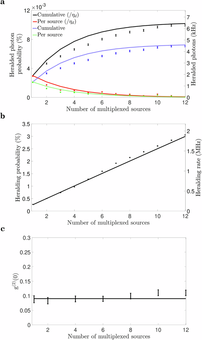
a Heralded single-photon probability and rate as a function of the number of multiplexed sources N, where dashed lines represent detected probabilities and rates, and straight lines correspond to values corrected for detector efficiency ηd (achieved by dividing by ηd). The contribution from each source, shown in green (detected) and red (corrected), decreases exponentially as photons in the mth time-bin must traverse the loop m − 1 times, experiencing a 1.47 dB loss per round trip. b Heralding detection rate and probability versus N. c Second-order autocorrelation function g(2)(0) as a function of N. Both heralding probability and heralded detection probability are enhanced as N increases, while g(2)(0) remains unchanged. Solid line indicates the measured value of g(2)(0) of non-multiplexed source. Error bars are estimated assuming Poissonian error statistics.
In order to quantify unwanted multi-photon contributions, we measured the second-order correlation function g(2)(0) as a function of N, and found that it remains constant, as is shown in Fig. 2c. The observed value of g(2)(0) < 0.5 is consistent with the characteristic of a single-photon emitter, serving as a key verification of our design. These outcomes indicate that our time multiplexed source successfully enhances the single-photon generation probability within the recovery time of the detector without increasing the multi-photon contamination relative to the single photon fraction.
Due to imperfect matching between the photon storage loop and the laser repetition period, output photons become temporally distinguishable when generated in different time bins. However, our TFLN loop does not disturb spectral-temporal mode purity, as shown by autocorrelation measurements conducted as a function of round trips (see Fig. S4 in Supplementary Note 3). Nevertheless, our system is well-suited for single-photon-based quantum key distribution22, where photon indistinguishability is not required, but increasing photon probability boosts the secret key rate.
The light into and out of our TFLN chip is butt-coupled using tapered fiber lenses, with a coupling efficiency of approximately 3 dB per facet. The net transmission efficiency of the storage medium itself is 0.41, including one pass through the switch, before reaching the collection fiber. Therefore, net system efficiency of heralded photons is estimated to be ηs = 0.0225. This improves heralded single-photon probability for multiplexed source to pm = 0.021%, resulting in heralded single-photon rate of 13 kHz.
Discussion
We expect that our demonstrated source can be significantly improved with currently available technologies. For precisely and efficiently heralding only single-photon states and removing the contributions of multi-photon states, high-efficiency photon number detectors can be introduced. Additionally, classical photonics engineering can increase the overall efficiency of the entire system. By incorporating state-of-the-art components with achievable coupling losses for TLFN, one can expect impressive performance. These include a silicon propagation loss of 0.027 dB/cm23, an on-chip asymmetric Mach-Zehnder interferometer filter to separate idler and signal photons (with a loss of less than 0.1 dB)6, and off-chip filters to remove spurious pump photons (~0.3 dB)6. Additionally, SiN couplers, which exhibit a loss of about 0.1 dB24, can be integrated on a silicon waveguide using a low-loss adiabatic taper (~0.02 dB loss)25. With state-of-the-art detector efficiencies approaching unity26,27, the system is expected to achieve a heralding efficiency of ηi = 0.89 and a net heralded efficiency of ηs = 0.87, including coupling to the TFLN chip (~0.1 dB loss). We assume that, given the similar values of refractive indices of SiN (nSiN ≈ 2) and LN (nLN ≈ 2.1), the coupling losses for TFLN will be comparable to those for SiN. Moreover, spectral indistinguishability can also be improved through alternative methods, such as employing inter-modal SFWM to suppress side lobes of a joint spectral amplitude represented by a sinus cardinal, achieving 99% spectral indistinguishability28.
The primary limitation of achieving a higher E in single-photon probability is directly related to losses experienced by heralded photons during TFLN storage, including switch losses. A recent demonstration has significantly reduced TFLN propagation loss, achieving a state-of-the-art, record-low loss of 0.013 dB/cm29. This advancement enables the effective multiplexing of 300 time bins, reducing the operation rate R to 16.66 MHz, increasing the enhancement factor E to 57. We can predict how scalable our system, i.e. generating several individual photons simultaneously, with state-of-the-art waveguide loss and with the feasible improvements outlined above by calculating ({C}_{n}={p}_{m}^{n}R), denoting an n-photon coincidence rate. In the low-squeezing regime where μ ≈ g(2)(0) = 0.01, the output probability of a multiplexed source would be pm ≈ 0.45. Therefore, the source is readily applicable even for n≥10 photons, with reasonably high event rates of C10 ≈ 5.7k s−1. On the other hand, a hybrid spatial (M sources) and temporal (N modes) multiplexing setup, based on a logarithmic tree structure—where each photon traverses the (lossy) switch (lceil {log }_{2}(M)rceil) times followed by temporal multiplexing in a TFLN medium, achieves higher performance using state-of-the-art components. For M = 4 silicon photon pair sources, pumped simultaneously and tuned to a low photon pair emission probability of μ ≈ g(2)(0) = 0.01, and with N = 150 time bins, the probability pm reaches 0.7 with E = 92. For M = 8, the probability pm further increases to 0.78 with E = 103. In Supplementary Note 5, we discuss the envisioned on-chip implementation of a hybrid spatial and temporal multiplexed single-photon source.
In summary, we have demonstrated a temporal multiplexing scheme utilizing TFLN photonics for the efficient enhancement of single-photon generation. Our system, operating at 62.2 MHz, achieved a factor of 3.37 ± 0.05 enhancement of the base probability rate, with negligible change to the second order correlation function g(2)(0) as a function of the number of multiplexed source N. This demonstration, highlighting the feasibility and potential of TFLN photonics, paves the way for creating near-deterministic single-photon sources using a resource-efficient and hence scalable multiplexing scheme. A complete comparison with other relevant works on temporally multiplexed photon sources is included in Supplementary Note 1. Incorporating currently available technologies with our scheme can further boost the output photon probability, providing a valuable resource for burgeoning large scale quantum technologies.
Methods
Experimental method
A 1.2 cm-long on-chip silicon waveguide source is pumped by N sequential bright pump pulses (1545 nm, 6 ps pulse duration) with a period of τ = 200 ps. The pulses are selected from a 10 GHz repetition rate erbium glass oscillator laser and then amplified through an EDFA before illuminating the waveguide via a grating coupler to probabilistically generate photon pairs through SFWM. This process occurs every 16.07 ns. Such a novel pumping scheme defines a high output clock rate of the multiplexed source as R = 62.2 MHz, so that the multiplexing within the recovery time of the detectors can be achieved. Therefore, in our multiplexing setup up to N = 80 time bins do not come at the cost of any reduced rate R. The generated single photons are separated using off-chip WDM filters at energy-conserving wavelengths of 1540.56 nm (0.22 nm, Opneti) and 1550.12 nm (0.22 nm, Opneti), defining the herald and the heralded single-photon channels, respectively. The herald photons are directed to a SNSPD (Quantum Opus) and recorded by a time-tagger (qutools quTAG) to generate timing data for the detection events. Subsequently, the heralded photons are coupled to a high-resolution single-photon buffer based on low-loss TFLN photonics. The TFLN device, capable of resolving 200 ps time-steps, includes a 2.4 cm-long loop and a 0.4 cm-long Mach-Zehnder electro-optic switch in push-pull operation mode, featuring a 3-dB electro-optic bandwidth exceeding 40 GHz30 (see Supplementary Note 3 for more details). The measured fiber-to-fiber insertion loss, including coupling, is below 6.8 dB.
The FPGA state machine, clocked by the laser, serves a dual role: it controls detect-capture-release logic and generates a carving signal for pump pulse selection (See Supplementary Note 4 for further details). The carving signal, generated by the FPGA, is amplified and fed into the VOA to select the pump pulses. The clocked switch control pulse, emitted by the FPGA, is fed into an UC (Analog Devices HMC674LP3E) to achieve a fast fall-rise time (approximately 20 ps). Following this, it undergoes amplification through a broadband EA to match Vπ (approximately 6V) of the TFLN switch before being applied to the device through high-speed radio frequency probe arms via micropositioners. This process acts to store the heralded photon for the necessary integer multiples of τ in the TFLN loop until the predetermined output time-bin, i.e., the final time-bin defined by the pump laser pulse train. To compensate for the time required to route the heralding photon to the detector and the electronic signal announcing the detection event back to the FPGA, a static fiber delay of T approximately 400 ns is introduced into the heralded path to ensure activation of the switch on the same clock cycle. A variable ODL featuring ps resolution is responsible for fine alignment between the heralded photons and electrical switch signals to achieve precise synchronization.
TFLN device design and fabrication
The proposed device design utilizes a commercial TFLN platform, incorporating a 360 nm thick x-cut LN thin film to take advantage of the largest electro-optic tensor component r33 of LN. The thicknesses of the buried oxide layer is 15 μm. Utilizing the x-cut TFLN configuration allows for the traveling wave electrodes of the modulator to be positioned on the sides of the waveguides and be simply fabricated by lithography and liftoff process. To achieve a large bandwidth, capacitance-loaded traveling-wave electrodes are employed, with a length of 0.4 cm. This design choice increases the device’s bandwidth significantly (See Supplementary Note 3 for more detailed information).
Multiplexed source
The maximum attainable single photon generation probability enhancement E is determined by the losses in the storage loop. With an increase in the number of time bins available for multiplexing, beyond a certain point, each additional unit of input results in a smaller increase in output probability, resulting in a saturation in E. Given this consideration, our device is suitable for temporal multiplexing with a limited number of time bins, N = 12, as the round-trip loss of our loop averages approximately 1.47 dB, including one pass through the switch.
Responses