Secure implantable cardiac pacemaker for medical consumer electronics

Introduction
The field of medical electronics includes life support instrumentation, patient monitoring, hearing aids, diagnostic equipment for measuring, monitoring, and recording body functions such as heartbeat and brain waves1. Hardware IPs are crucial components of such medical electronic systems as they enable better performance and efficacy. Therefore, the demand of hardware IPs in different domains is always escalating2,3,4,5,6,7 Specifically in electronic medical devices, both internal and external to the human body, reliable hardware IP functioning is critical to the safety of the end user (patient). Further, a patient’s demand for improved life quality has driven the necessity of sophisticated implantable medical devices to grow briskly over the last few years. Cardiac pacemaker is one such implantable electronic medical device that is implanted into the patient body for maintaining the normal cardiac activity. In a typical cardiac pacemaker, computationally intensive algorithms for pulse signal filtration (through filter bank) and QRS complex (R wave) detection are present8,9,10, Therefore, it is crucial to design their respective dedicated hardware IPs.
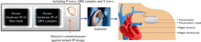
Motivation for securing cardiac pacemaker hardware IPs for the benefit of heart patient: quality, reliability, and safety are the most significant objectives for equipment manufactured in the medical market segment. More explicitly, consumer medical systems before being implanted into human must pass through more stringent quality checks and tests than other electronic systems used in military applications etc. in order to ensure safety. Further, in the globally deployed supply chain, the process for designing the medical electronic devices irrespective of their domain (for example consumer electronics, healthcare and automotive vehicle), involves untrustworthy offshore entities. The involvement of such various untrustworthy offshore entities, substantially upsurges the risk of IP piracy11,12,13,14,15,16,17 Therefore, before the integration of hardware IPs (imported from untrusted IP vendors) in system-on-chip of implantable pacemaker devices, it is vital to ensure their authenticity at the pacemaker system design house at the system-on-chip (SoC) integrator level. This is because fake/pirated IPs of cardiac pacemaker may not undergo quality/reliability checks and are hazardous. Pirated IP inside cardiac pacemaker may lead to misclassification or wrong detection of heart’s rhythmic activity and may thereby produce irregular (mistimed) pulse from the cardiac pacemaker. This could lead to fatal consequences to the patient. Further, once surgically implanted into human body, replacement of pirated IP from cardiac pacemaker device (as a corrective measure) is not easily possible without nonsurgical procedure. Therefore, it becomes mandate to detect and isolate such pirated IP designs before incorporation in pacemaker devices for safeguarding patients. This therefore mandates the need of designing secure hardware IPs for cardiac pacemaker with detective countermeasure capability against pirated versions. Hence, it falls upon the SoC integrator to guarantee the safety by detecting IP piracy5,6,18,19 To identify illicit design versions effectively, the inclusion of a covert security mark can be instrumental in enhancing detective control and isolation.
The approach introduces the following novel contributions: (a) a novel secure hardware IP designs for filter bank and QRS complex detector for cardiac pacemaker. (b) a novel secure design flow using AES-256 secret signature for generating secure version of hardware IPs for implantable cardiac pacemaker against IP piracy. This ensures robust security by facilitating the identification and segregation of vulnerable hardware IPs before integration into implantable pacemakers, which otherwise may lead to fatal consequences for the patients. (c) the proposed approach presents novel secure high level synthesis methodology that is capable to generate secure RTL datapath design for filter bank and QRS complex for implantable cardiac pacemaker. (d) the secure hardware IP design generated using proposed approach ensures higher robustness and safety in terms of lower stronger digital evidence for piracy detection (probability of coincidence) and strong robustness against brute force attack (tamper tolerance) compared to secure hardware IP design with, watermarking18, automatic signature insertion19, digital signature5 and hardware steganography6.
Results and analysis
The results of the presented methodology for generating the secure hardware IP cores for implantable cardiac pacemaker are analyzed in this section. Further, the security strength and the design cost of presented framework is evaluated for several other hardware IP core security techniques in the state-of-the-art. The system configuration utilized to execute the proposed approach includes an Intel processor core2 duo, 2.10 GHz RAM -3GB.
Security analysis in terms of probability of coincidence and tamper tolerance
The proposed design methodology achieves robust security against the threats of IP piracy, because exact regeneration of encoded hardware security constraints corresponding to encrypted signature is impossible. From the perspective of a potential attacker, the task involves deciphering various secret information elements discussed in section IV.C, which play a pivotal role during the generation and implantation of signatures. These elements are exceedingly challenging to compute mathematically, as indicated by the high entropy of the proposed approach. Essentially, this means that all these critical security details can only be decoded by a legitimate IP vendor.
The security provided by implanting the encrypted signature into the hardware IP designs is assessed using the following security metrics including probability of coincidence (Px): This metric indicates the strength of digital evidence. Tamper Tolerance (TT): Signifying the design’s resilience against tampering attacks. Entropy: Measuring the amount of uncertainty or effort required for an attacker to determine the value of the secret mark.
‘Px’ denotes the probability of coincidentally detecting security constraints that were generated using the proposed methodology in an unsecured design. This probability is considered a measure for detecting the digital evidence in a non-watermarked design (false positive). Therefore, lower the probability, stronger is the digital evidence corresponding to a genuine IP vendor. The strength of digital evidence embedded or robustness against false positive is evaluated in terms of following metric5,6,18,
Where, ‘({{rm{R}}}_{{rm{s}}})’ corresponds to the count of storage elements (registers) needed to store all the storage variables (including inputs and outputs of functional units) of the hardware IP design before the incorporation of encoded hardware secret security constraints and ‘T’ stands for the quantity of implanted secret hardware security constraints, which are generated based on the encrypted signature, encoding algorithm, and the ordering of storage variables as specified by the original IP vendor. To ensure robust detective countermeasure or to achieve lower Px, larger number of security constraints should be implanted into the IP design. The Px achieved through proposed methodology corresponding to hardware IP design for QRS complex has been reported for varying encrypted encoded constraints size, as shown in Table 1. As apparent from Table 1, increase in the number of security constraints results into lower Px value. Further, the comparison of Px value corresponding to proposed secure hardware IP design of QRS complex embedded with encrypted signature with proposed secure hardware IP design of QRS complex embedded with refs. 5,18,19, and ref. 6 is depicted in Table 2 and with ref. 20 and ref. 7 is shown in Table 3. As apparent, the proposed methodology secured with AES signature attains lesser ‘Px’ compared to proposed designs secured with refs. 5,6,18,19,20 and ref. 7. This is due to the fact that the proposed methodology empowers the IP vendor to create and embed a greater number of concealed hardware security constraints into the design, in contrast to other proposed design approaches5,6,18,19,20 and ref. 7. Further, Px comparison of proposed secure hardware IP design for filter bank, is shown in Table 4.
Tolerance against tampering attack using brute force is analyzed using the tamper tolerance ability of the approach. Therefore, it is desirable to achieve larger key-space, in order to hinder an attacker from finding the exact hidden signature to tamper. The tamper tolerance is assessed through the following function5,18,
Where, ‘β’ represents the number of encoding digits of the generated encrypted signature. Because the proposed approach generates a substantially larger number of security constraints for embedding into the design using AES encryption, it consequently leads to a more robust tamper tolerance. The TT of the presented approach for varying size of implantable encoded hardware security constraints is depicted in Table 1. As evident, the strength of tamper tolerance increases with a greater number of implantable security constraints in the hardware IP design. Further, the comparison of strength of tamper tolerance of the proposed approach with AES as compared to proposed approach with refs. 5,6,18,19 respectively, is shown in Table 5 and with ref. 20 and ref. 7 is shown in Table 6. As evident the tamper tolerance ability of the proposed approach with AES is considerably larger due to production of more encoded security constraints corresponding to generated encrypted signature as compared to proposed approach with refs. 5,6,18,19,20 and ref. 7 respectively. Further, TT comparison of proposed secure hardware IP design for filter bank, is shown in Table 4.
Security analysis in terms of entropy
The entropy (({E}_{T})) can be defined as the measure of amount of effort required for an attacker to determine the exact combination of the secret mark (security constraints), as per NIST21. This effort required (in terms of probability) from an adversarial perspective to exactly guess the hidden signature combination can be quantified as: ({E}_{T}=1/{2}^{{rm{mu }}}), where ‘μ’ corresponds to the strength of the signature and ({2}^{{rm{mu }}}) is the exhaustive signature space. For example, if the value of ‘μ’ is 2176 bits, then the value of ‘({E}_{T})’ is 9.0934E−656. Hence, to evaluate the entropy of the proposed approach in terms of the total effort (TE) required from an adversarial perspective, it can be assessed as follows22,23,
where ‘K’ is the size of encryption key and ‘L’ is the size of input signature before encryption. Therefore, the larger the value of μ, K and L, higher is the effort required for guessing the exact signature combination from an attacker’s perspective. Table 7 displays the entropy of the proposed approach with AES, as measured in terms of the difficulty of adversarial guessing and the effort required, corresponding to varying signature sizes. In addition to, the comparison of entropy of the proposed approach for generating secure QRS complex hardware IP design embedded with encrypted signature is compared with proposed secure QRS complex hardware IP design embedded with refs. 5,6,7,18,19,20 is shown in Table 8. As evident, the proposed approach achieves stronger entropy (lesser probability value) than refs. 5,6,7,18,19,20
Design cost analysis
The design cost Cd(Rh), for generating the secure hardware IP design for implantable cardiac pacemaker (pre and post-embedding the generated encoded secret hardware security constraints corresponding to encrypted signature using AES) is evaluated using the following design metric5,6,18,
Where, ({{rm{R}}}_{{rm{h}}}) represents the resource constraints of the design (obtained from design space exploration process), ‘({{rm{{Upsilon }}}}_{d})’ and ‘({{rm{alpha }}}_{d})’ signify latency and area of the design, respectively, ({{rm{{Upsilon }}}}_{m}) and ({{rm{alpha }}}_{m}) denote the maximum design latency and area. ({{rm{lambda }}}_{1}) and ({{rm{lambda }}}_{2}) corresponds to the weighing factors of normalized latency and area in the design cost function. The computation of latency and area for the proposed secure hardware IP design for an implantable cardiac pacemaker is based on a 15 nm open-cell NanGate library24. The design cost for generating secured hardware IP for the QRS complex using the proposed approach is presented in Table 9. As apparent from Table 9, the proposed approach does not impose any additional design cost overhead post-embedding the produced larger security constraints with respect to encrypted signature of specified length (by genuine IP vendor). This is because during the embedding process of security constraints into the design, the proposed methodology does not incur any extra storage element (registers) for accommodating the locally altered storage variables. Table 10 shows the performance comparison of filter bank and QRS complex IP designs with and without the proposed method in terms of accuracy of signals generated. Without the proposed AES embedded signature, the pirated IP versions of filter bank and QRS complex may contain malicious Trojan logic (performance degradation-based hardware Trojan (PD-HT) logic). As discussed earlier, pirated IPs do not undergo rigorous testing and quality checks, therefore possibility of PD-HT is highly likely as established in the literature25. Table 10 presents a simulated case study of filter bank and QRS complex IP designs with AES signature and without AES signature (pirated version containing PD-HT malicious logic). The pirated IP designs due to PD-HT logic incurs performance degradation in terms of execution delay (in our results we consider a number of invertors (L) equals to 10 as part of the PD-HT logic). However, the proposed IP design with AES is authentic and does not contain PD-HT malicious logic. Therefore, the execution delay reported for proposed secure IP designs does not incur any delay due to absence of malicious logic. Moreover, the tradeoff between security (Px) and design cost for the proposed secure hardware IP design for the QRS complex, as it relates to the varying strength of embedded security constraints, is illustrated in Fig. 1. Furthermore, Fig. 2 illustrates the tradeoff between security (Px) and design cost for the proposed secure hardware IP design for the filter bank. This tradeoff varies with the strength of embedded security constraints. This analysis ensures the robustness of the security in the proposed hardware IP design by making it increasingly difficult for an adversary to detect the authentic signature in an unsecured design version. As a result, it portrays the presence of stronger digital evidence. We have also analyzed the proposed secure IP designs in terms of Cyclone IV FPGA resources (layout is shown in Fig. 3). Moreover, Fig. 4 shows the area of the proposed QRS complex and filter bank IP designs in Secure Cardiac Pacemaker in terms of Cyclone IV GX FPGA Logic Elements (LE) based on RTL synthesis executed in Intel Quartus tool v13.1. As evident, secure QRS complex IP design being a more complex design with significantly larger number of RTL components consumes more logic resources in Cyclone IV FPGA, compared to filter bank IP design that occupies lesser RTL components. Additionally, Fig. 5 shows the area of register hardware of QRS Complex IP design in terms of Cyclone IV GX FPGA LE (before and after AES signature embedding). As evident from Fig. 5, there is no area overhead in terms of FPGA resources in proposed secure QRS Complex IP design, compared to without AES embedded QRS Complex IP design. Further, Fig. 6 shows the area of register hardware of filter bank IP design in terms of Cyclone IV GX FPGA LE (before and after AES signature embedding). As evident from Fig. 6, there is no area overhead in terms of FPGA resources in proposed secure filter bank IP design, compared to without AES embedded filter bank IP design. Additionally, Figs. 7 and 8 report the power consumption of the proposed secure IP designs (filter bank and QRS complex) in terms of interconnect logic power, storage hardware power and power consumed by functional units.

This illustrates tradeoff between security (Px) and design cost for the proposed secure hardware IP design for the QRS complex, as it relates to the varying strength of embedded security constraints.

This illustrates the tradeoff between security (Px) and design cost for the proposed secure hardware IP design for the filter bank.
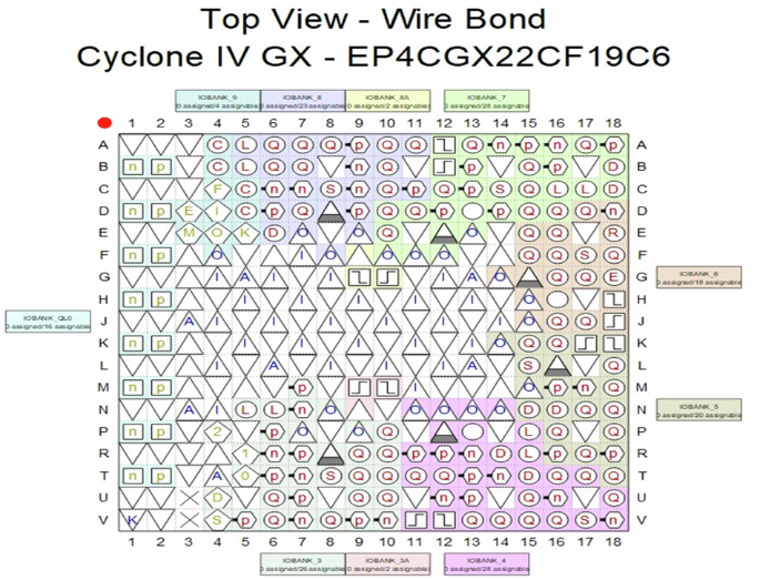
This presents the proposed secure IP designs in terms of Cyclone IV FPGA resources.
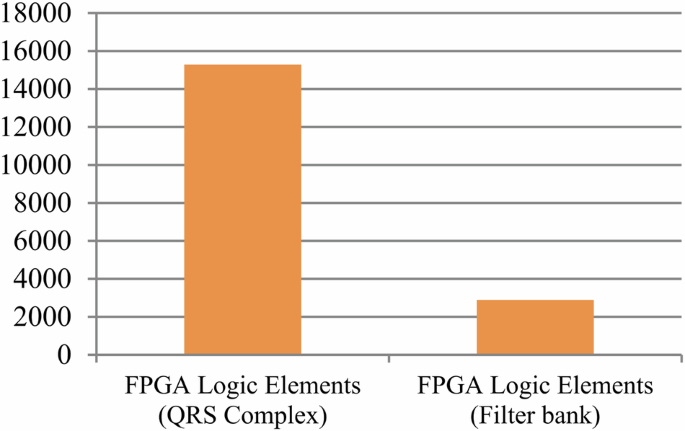
Area of proposed QRS complex and filter bank IP designs in secure cardiac pacemaker in terms of cyclone IV GX FPGA logic elements based on RTL synthesis executed in Intel Quartus tool v13.1.
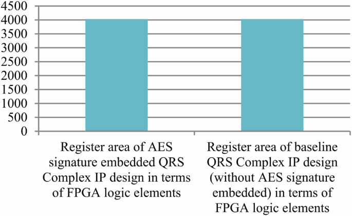
Area of register hardware of QRS Complex IP design in terms of Cyclone IV GX FPGA LE (with and without AES signature embedding).
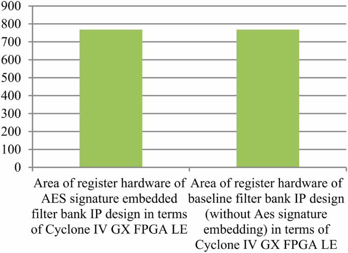
Area of register hardware of filter bank IP design in terms of Cyclone IV GX FPGA LE (with and without AES signature embedding)
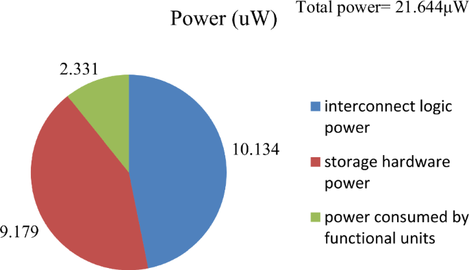
Analysis of power consumption of the proposed secure filter bank IP design based on required interconnect logic, storage hardware and functional units
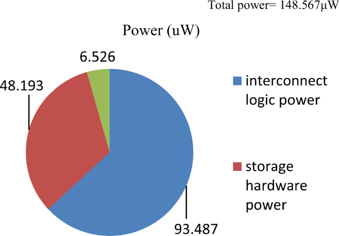
Analysis of power consumption of the proposed secure QRS complex IP design based on required interconnect logic, storage hardware and functional units
Therefore, these embedded encrypted encoded security constraints (of IP vendor’s AES signature) empower a SoC integrator with robust detective control against pirated design versions, thereby enabling their sturdy isolation before integrating into an implantable cardiac pacemaker device for safety of end user.
Discussion
Background on cardiac pacemaker
Cardiac pacemaker is a crucial implantable device used for detecting, monitoring and maintaining the normal heart rate and rhythm of a patient. It monitors the incoming pulse trough pacemaker lead and produces pulse accordingly. If pacemaker encounters any abnormality in the cardiac cycle, then it generates controlled electrical impulses to specific chambers (atrium and/or ventricle) of heart to restore or maintain the normal heartbeat rhythm26. A cardiac cycle is characterized as the recurrent sequence of heart waves including P wave, QRS complex and T wave as depicted in Fig. 9. Further, QRS complex comprises of Q, R and S waves. During the monitoring of cardiac rhythm, R-R interval of two consecutive R waves is analyzed. Therefore, precise and accurate monitoring of QRS complex is crucial for assuring the normal cardiac rhythm of the heart26,27,28,29,30 This is because, rhythmic activity may be affected by various types of noises such as electromyographic (EMG) interference (muscle contraction and relaxation signals may lead to a deterioration in the signal-to-noise ratio), respiration may also cause baseline drift and a composite noise generated through the combination of these noises30. Further, each cardiac cycle has two phases named systole and diastole. In the systolic phase of cardiac cycle, heart chambers (the lower chambers; right and left ventricle) pumps the blood flow towards the periphery via arteries. While during the diastolic phase, heart chambers (the upper chambers; right and left atrium) are filled with incoming blood from the veins.

A cardiac cycle is characterized as the recurrent sequence of heart waves including P wave, QRS complex and T wave.
Related works
In the literature, few approaches have been presented for detecting and monitoring the rhythmic activity for cardiac pacemaker. In the approach31, a field programmable gate-array (FPGA) based peak (R wave) detection technique for cardiac pacemaker was proposed. Further in ref. 32, an FPGA based model of QRS complex detection is presented based on the Pan and Tompkins algorithm that enables the heart rate detection and monitoring. In ref. 33, an FPGA implementation was presented to investigate nonlinear dynamics of cardiac pacemaker model represented by using the method of harmonic balance and the method of multiple time scales. In ref. 34, an FPGA based pulse generator system was implemented. In this approach, Dynamic Partial Reconfiguration (DPR) property of FPGAs has been exploited for performing remote change in operational mode of the pacemaker. The approaches31,32,33,34 presented FPGA based implementation for performing cardiac pulse investigation. However, none of these approaches have targeted to design hardware IPs for implantable cardiac pacemaker. Further, none of the approaches31,32,33,34 have considered designing secure hardware IPs of filter bank and QRS complex for cardiac pacemaker device using secure HLS embedded with AES encrypted signature14. Further Srivastava et al.35, presented a hardware implementation of rate-adaptive dual-chamber pacemaker (RDPM) using a piezoelectric sensor. Rate adaptive pacemaker sense the patient’s activity through special sensors controls the pacing rate according to the patient’s activity. However35, did not design hardware IPs for filter bank and QRS complex as well as did not design the secured version of the same, unlike proposed approach using HLS. On the other hand, in approach36, A proposal was made for the development of a low-power analog integrated circuit design aimed at enhancing ECG acquisition systems by means of miniaturization and system integration. In this approach, an efficient low-potable analog front-end system was introduced, consisting of an ECG signal acquisition board, an on-chip low-pass filter, and an on-chip successive approximation analog-to-digital converter. These components are designed to be integrated into portable ECG detection devices for signal acquisition. All these approach31,32,33,34,35,36 do not present secure hardware IP designs for filter bank and QRS complex for implantable cardiac pacemaker unlike proposed approach which presents secure hardware IP designs for both using HLS. The proposed approach presents the secure hardware IP RTL designs using proposed secure HLS methodology embedded with AES-256 signature. The proposed design methodology is capable of ensuring the robust security through detection of pirated design versions before integrating into cardiac pacemaker device, thereby ensuring safety of end user. Further in the literature, some IP core protection approaches for hardware security have been presented such as hardware watermarking18, automatic signature insertion19, digital signature5, hardware steganography6 palmprint20 and facial biometric7. In the watermarking approach18, a binary encoding scheme is employed for implanting watermarking constraints for intellectual property protection. In this approach firstly, the vendor’s signature is transformed into watermarking constraints based on binary (0 and 1) encoding. These constraints are subsequently added into the design (in the form of additional edges into the color interval graph). The added edges represent the watermark of the vendor. In ref. 19, a watermarking scheme was presented which relies on inserting the digital signature bits at the hardware description language (HDL) design level based on system resources. In this approach, security of the associated watermark signature is protected using message-digest (MD)-5 and secure hashing algorithm (SHA)-1 but incurs design area overhead. Further, in approach5, a digital signature based watermarking mechanism was presented for IP core protection. This employs SHA for generating bitstream digest and performs Rivest–Shamir–Adleman (RSA) based encryption. Moreover, a hardware steganography-based security method was introduced for the detection of unauthorized versions of DSP IPs prior to their integration into consumer electronics (CE) systems6. In this approach, hidden steganographic mark is inserted into the DSP design. Additionally, the quantity of concealed digital evidence intended for embedding is entirely adjustable by the designer, utilizing a ‘thresholding’ parameter. The intricate process of generating stego-constraints through a secret stego-key makes it more robust compared to watermarking. Nevertheless, if an adversary gains access to information about stego-key or parameter of entropy threshold, it may affect the security as evasion during IP piracy detection is possible. Further20, and7 presented biometric signature driven approaches. Both these approaches do not employ signature encryption and are not capable of generating large number of security constraints. On the contrary, the proposed approach with AES-256 generates secure hardware IP designs that provides detective control against pirated versions and enables isolation of such fake versions before integration into implantable cardiac pacemaker devices. This is due to the fact that the proposed methodology has the capability of generating and implanting large size digital evidence (covert hardware security constraints) into the design at zero design cost overhead than related approaches5,6,18,19 thereby providing lower probability of coincidence (false positive), stronger tamper tolerance (against brute force attack) and stronger entropy (indicating higher adversarial effort in guessing the exact security constraints).
Method
The proposed approach for generating the secure hardware IPs for implantable cardiac pacemaker has been discussed in subsequent subsections.
Overview and motivation
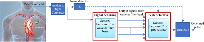
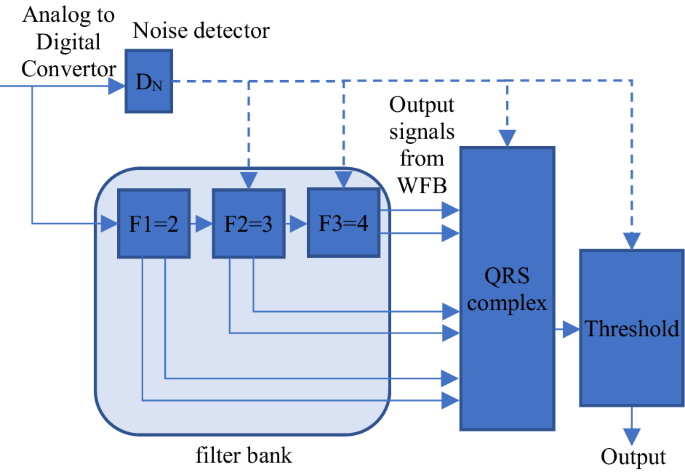
A cardiac pacemaker comprises of different components including analog to digital convertor, noise detector, wavelet filter bank (WFB), QRS complex detector and threshold function for maintaining the normal rhythmic functionality of the heart. Analog to digital convertor, converts the incoming pulse from pacemaker lead into digital form. Further, wavelet filter bank decomposes the input pulse into sub bands which are subsequently fed as input to the QRS complex detector. QRS complex detector, detects the R wave to analyze the rhythmic activity of the heart pulse through generalized likelihood ratio test (GLRT). The threshold function is responsible for distinguishing whether the incoming pulse should be classified as cardiac activity or noise, depending on the threshold value. This process continues for each incoming pulse30. The thematic representation of the proposed methodology for secured hardware IPs for implantable cardiac pacemaker is shown in Fig. 10. The proposed methodology generates secure hardware IPs for filter bank and QRS detector used in implantable cardiac pacemaker through high-level synthesis process. In order to do so, firstly the transfer function of QRS complex detector and filter bank are transformed into control data flow graph (CDFG). Subsequently, the generated scheduled CDFGs with register allocation are exploited for covertly implanting the secret hardware security constraints resulting through encoding the encrypted signature from AES-256, during HLS. Subsequently, post performing the datapath synthesis, RTL structure for secured hardware IPs is obtained.
The proposed methodology generates secure hardware IPs for filter bank and QRS detector used in implantable cardiac pacemaker through high-level synthesis process.
These hardware security constraints post implantation facilitate detective control against pirated IPs. The effectiveness of a robust and smooth detective control system is paramount in addressing counterfeit component issues, because pirated components are unreliable, hazardous and may contain malicious logic causing irregularity in pulse generation. Further once implanted, it is not possible to replace the pirated/counterfeited hardware IPs of pacemaker without nonsurgical procedures. Such pirated unsecured hardware IPs integrated in implantable pacemakers may lead to fatal consequences for the patients. Therefore, ensuring the integration of only authentic hardware IPs (at the SoC integrator level) into implantable cardiac pacemakers safeguards the end user (patient).
The overview of the proposed secured hardware IP cores for a cardiac pacemaker is shown in Fig. 11. In a cardiac pacemaker, ADC and noise detector are the analog components. On the other hand, filter bank and QRS complex detector are the two applications which are computationally intensive in nature. Therefore, dedicated secured hardware IPs are designed for both these components. As evident from Fig. 11, the proposed hardware IPs are secured against piracy from an adversary. The proposed design scheme ensures the authenticity of the integrated hardware IP cores, by enabling the isolation of pirated components through robust and seamless detective control against piracy at the pacemaker design house (at the SoC integrator level).
In a cardiac pacemaker, ADC and noise detector are the analog components. On the other hand, filter bank and QRS complex detector are the two applications which are computationally intensive in nature. Therefore, dedicated secured hardware IPs are designed for both these components.
Details of the proposed secure hardware IP cores for cardiac pacemaker
The details of the methodology for designing the secure hardware IPs for QRS complex and filter bank of cardiac pacemaker is discussed in subsequent subsections.
Cardiac pacemaker with filter bank and QRS complex
A cardiac pacemaker, comprises of filter banks as a wavelet decomposer and QRS complex, which are the computationally intensive counterparts in order to perform accurate pulse detecton and enabling normal heart rythm. Post receiving the pulse signal from pacemaker lead, it propogates to filter bank via ADC. Filter bank decompose the input pulse signal into sub bands with two outputs as Wi and Wi+1 corresponding to monophasic and biphasic morphologies. The filter bank comprises of three branches (F1 = 2), (F2 = 3) and (F3 = 4), that are responsible for scaling and filtering the pulse signal as shown in Fig. 12. This is because to cover the frequency spectrum of an R wave, three scales are sufficient37. Further, filter bank output is defined as:
Where, X(n) is the input to the filter bank and H is defined as the matrix formed by linear combinations of representative functions which is computed using Mallat’s algorithm38. Finally, as shown in Fig. 13, the decision signal Z(n) is computed by a generalized likelihood ratio test (GLRT) as follows39:
Where,
The filter bank comprises of three branches (F1 = 2), (F2 = 3) and (F3 = 4), that are responsible for scaling and filtering the pulse signal.

The decision signal Z(n) is computed by a generalized likelihood ratio test (GLRT)
The component ({left({{rm{H}}}^{{rm{T}}}{rm{H}}right)}^{-1}) in Eq. (2) is symmetric and sparse (comprising half of the elements as zero, as shown in Eq. (3) (adopted from ref. 39). Therefore, it eliminates the need for their implementation. Subsequently, the threshold level determines the existence of an R wave and signals to the pulse generator accordingly. Thus, GLRT with threshold function estimates the heart rate with the outputs of decomposed filter bank.
Generation of CDFG of Filter Bank and QRS Complex
The CDFG corresponding to filter bank and QRS complex are generated by transforming their mathematical description/transfer function. The transfer function function of employed low pass and high pass filter in the cardiac pacemaker filter bank is given as follows:
Transfer function of low pass filter:
Now, the above signal corresponding to low pass filter can be represented in time domain as follows (by applying the Z transformation):
Further, the transfer function of high pass filter:
Now, the above signal corresponding to high pass filter can be represented in time domain as follows (by applying the Z transformation):
Subsequently, the CDFG corresponding to low pass and high pass filters is derived as shown in Fig. 14, where, x(n) indicates the current input and x(n-1), x(n-2) and x(n-3) represents input values corresponding to previous stages and the integer values represent the filter coefficient.
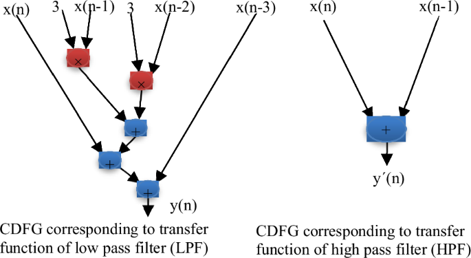
Here, x(n) indicates the current input and x(n-1), x(n-2) and x(n-3) represents input values corresponding to previous stages and the integer values represent the filter coefficient.
Further, the transfer function for QRS complex is obtained from (2), where the multiplication of y(n) with the first column of ({left({{rm{H}}}^{{rm{T}}}{rm{H}}right)}^{-1}) and the first element of ({{rm{H}}}^{{rm{T}}}{rm{X}}left({rm{n}}right)) is executed, where ({{rm{C}}}_{3{rm{k}}+{rm{j}},{rm{i}}}) are elements of ({left({{rm{H}}}^{{rm{T}}}{rm{H}}right)}^{-1}) and ({{rm{y}}}_{3{rm{k}}+{rm{j}}}({rm{n}})) the output of the filter bank, with K = 0,1 and j = 1,2,3. The CDFG corresponding to QRS complex is shown in Fig. 15, where ({{rm{C}}}_{3{rm{k}}+1,{rm{i}}}), ({{rm{C}}}_{3{rm{k}}+2,{rm{i}}}) and ({{rm{C}}}_{3{rm{k}}+3,{rm{i}}}) represents the coefficient of the matrix corresponding to first column (as shown in (3)) and ({{rm{Y}}}_{3{rm{k}}+1})(Z), ({{rm{Y}}}_{3{rm{k}}+2})(Z), ({{rm{Y}}}_{3{rm{k}}+3})(Z) and ({{rm{Y}}}_{{rm{i}}})(Z) represnts the outputs of the filter bank. Similarly, for the other GLRT block, their corresponding CDFG is constructed. Finally, by performing the sum of these decomposed bands (GLRT outputs), pulse signal is constructed. It is then analyzed against threshold function to determine whether the incoming pulse is adjudged as a cardiac signal or as noise. The CDFG corresponding to QRS complex requires a total of 41 operations including 24 multiplications and 17 additions.
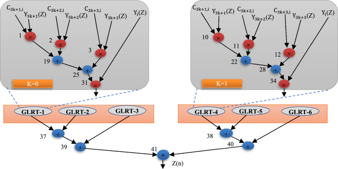
Here, the multiplication of y(n) with the first column of ({left({{bf{H}}}^{{bf{T}}}{bf{H}}right)}^{{boldsymbol{-}}{bf{1}}}) and the first element of ({{bf{H}}}^{{bf{T}}}{bf{X}}left({bf{n}}right)) is executed, where ({{bf{C}}}_{{bf{3}}{bf{k}}{boldsymbol{+}}{bf{j}},{bf{i}}}) are elements of ({left({{bf{H}}}^{{bf{T}}}{bf{H}}right)}^{{boldsymbol{-}}{bf{1}}}) and ({{bf{y}}}_{{bf{3}}{bf{k}}{boldsymbol{+}}{bf{j}}}({bf{n}})) the output of the filter bank, with K = 0, 1 and j = 1, 2, 3
Designing secure hardware IPs for implantable cardiac pacemaker
In order to design the secure hardware IPs corresponding to filter bank and QRS complex for implantable cardiac pacemaker, a secure high level synthesis methodology is proposed. The design flow for the same has been depicted in Fig. 16. In the proposed design methodology for generating secure hardware IPs for cardiac pacemaker, the primary inputs are module library, cardiac pacemaker application and resource constraints. Initially, in the pre-processing phase of HLS, the transfer function of filter bank and QRS complex is extracted from the input application (cardiac pacemaker) as discussed in subsection B.2). Susequently, their corresponding CDFGs are costructed as shown in Figs. 14 and 15. Thus, in HLS pre-processing phase, CDFGs corrresponding to filter bank and QRS complex are generated. Subsequently, the CDFGs corresponding to filter bank and QRS complex are scheduled. The scheduling process accepts the following inputs: IP vendor specified resource constraints, scheduling algorithm and available dependency information of storage variables. In order to schedule a CDFG, firstly the optimal resource configuration are obtained from design space exploration process by considering the design constraints (area and delay)40. A LIST scheduling is applied which aims to schedule the maximal operations in a specific control step adhering to data dependency and resource constraints15. Subsequently, the hardware resources are allocated and their binding is performed. The scheduled CDFG corresponding to filter bank, post performing the resouce allocation and binding, is shown in Fig. 17. As apparent from Fig. 17, the scheduling has been performed based on the hardware resources one adder and one multiplier (obtained from design space exploration process) which requires six control steps for obtaining the final output value, where, I0-I13 are the storage variables and the registers needed to adjust the storage variables are designated using different colors. In the scheduled CDFG design corresponding to filter bank, eight registers are required. On the other hand, the scheduled CDFG corresponding to QRS complex, post performing the resouce allocation and binding, is shown in Fig. 18. As apparent from Fig. 18, the scheduling has been performed based on the resources two adders and three multipliers (obtained from design space exploration process) which requires twelve control steps (τ1-τ12) for obtaining the final output value, where, I0-I82 are the storage variables and the registers needed to adjust the storage variables are designated using different colors. In the scheduled CDFG design corresponding to QRS complex, 42 registers are required.

In the proposed design methodology for generating secure hardware IPs for cardiac pacemaker, the primary inputs are module library, cardiac pacemaker application and resource constraints. Initially, in the pre-processing phase of HLS, the transfer function of filter bank and QRS complex is extracted from the input application (cardiac pacemaker). Susequently, their corresponding CDFGs are constructed. Thus, in HLS pre-processing phase, CDFGs corrresponding to filter bank and QRS complex are generated. Subsequently, the CDFGs corresponding to filter bank and QRS complex are scheduled. The scheduling process accepts the following inputs: IP vendor specified resource constraints, scheduling algorithm and available dependency information of storage variables. In order to schedule a CDFG, firstly the optimal resource configuration is obtained from design space exploration process by considering the design constraints (area and delay). A LIST scheduling is applied which aims to schedule the maximal operations in a specific control step adhering to data dependency and resource constraints. Subsequently, the hardware resources are allocated and their binding is performed. Post performing the resource allocation and binding, register allocation information corresponding to filter bank and QRS complex is extracted in the register allocation stage of HLS. This register allocation information is exploited for subsequently implanting the secret hardware security constraints, in order to implant secret strong digital evidence for performing detective countermeasure against piracy.

This requires six control steps for obtaining the final output value, where, I0-I13 are the storage variables and the registers needed to adjust the storage variables are designated using different colors. In the scheduled CDFG design corresponding to filter bank, eight registers are required.
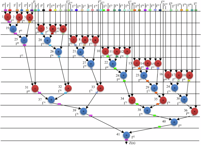
The scheduling has been performed based on the resources two adders and three multipliers (obtained from design space exploration process) which requires twelve control steps for obtaining the final output value, where, I0-I82 are the storage variables and the registers needed to adjust the storage variables are designated using different colors. In the scheduled CDFG design corresponding to QRS complex, 42 registers are required.
Post performing the resource allocation and binding, register allocation information corresponding to filter bank and QRS complex is extracted in the register allocation stage of HLS. This register allocation information is exploited for subsequently implanting the secret hardware security constraints, in order to implant secret strong digital evidence for performing detective countermeasure against piracy. In order to do so, signature implanting block accepts register allocation information corresponding to filter bank and QRS complex and the secret hardware secuity constraints to be embedded during register allocation phase of HLS. The secret hardware security constraints are generated by employing the encoding algorithm post generating the encrypted signature using AES-256. The details of the AES-256 mechanism are discussed in next subsection.
AES for generating secret hardware security constraints
The inputs to the AES are: (a) 256-bit input signature and (b) 256-bit encryption key, chosen by the original IP vendor. This results into an encrypted signature as output which is further encoded into its respective secret hardware security constraints. This produced covert hardware security constraints are implanted into the cardiac pacemaker hardware IP designs in register allocation stage of HLS. The AES algorithm encrypts the input signature with encryption key through the following:
-
Byte substitution layer: this is the initial layer that accepts the signature as its input and enhances the security of input signature by performing the non-linear transformation (confusion property) using S-box. The input signature bit is replaced to substitution process with the bits of S-box.
-
Diffusion layer: in this enhancement of security is done through using sub layers of diffusion process: a) shift rows b) mix column. The output of byte substitution acts as the input of the shift row function.
-
Key addition layer: this accepts the output of mix column diffusion layer and encryption key, as input. Subsequently, bitwise XOR operation is done through this encryption key to produce the output signature for the upcoming round of encryption. The byte substitution layer accepts the produced input for subsequent round of encryption.
-
Key scheduling layer: the encryption key is fed as an input to this layer for extracting the subkeys for the upcoming round. Using recursion process, the key for the next round is computed based on the previous round key value.
After the completion of encryption process for the initial signature, the encrypted signature is obtained. For instance, the encrypted signature obtained through AES-256, based on IP vendor specified 256-bit input and 256-bit encryption key, is as follows:
“10101110111010111001001111011110100110000010011110010010110000001000101100110001101111001011101101110011101001100111110000011101………….1100101111110001011101010001010111100011010111101000110011001111111000000101011110100101001000000010111101001”.
Therefore, post obtaining the encrypted digital template, it is converted into covert hardware security constraints. The hardware security constraints creation technique accepts the following inputs: scheduled CDFG of the application post resource allocation and binding (the scheduled CDFG of the corresponding design is responsible for dictating its storage variables), encrypted signature to be embedded, encoding algorithm and storage variable ordering (could be either sorted ascending order, sorted descending order, random order etc.). Note: An original IP vendor can specify/select the final encrypted signature strength to be embedded, can choose any of the several possible encodings for signature bits and also can select any of the possible ordering of storage variables. Further, assuming that signature bit 0 and 1 are encoded through the given algorithm:
-
For signature bit ‘0’: embed the security constraints indicating storage variable pair ‘(({{rm{I}}}^{{rm{x}}}) and ({{rm{I}}}^{{rm{y}}})) in case of QRS complex’ or ‘(({{rm{J}}}^{{rm{x}}}) and ({{rm{J}}}^{{rm{y}}})) in case of filter bank’ of even number required to be allocated to distinct registers, where ({{rm{I}}}^{{rm{x}}}) and ({{rm{I}}}^{{rm{y}}}) or ({{rm{J}}}^{{rm{x}}}) and ({{rm{J}}}^{{rm{y}}}) can be of any integer value with in the range of storage variables of the respective design and
-
For signature bit ‘1’: embed the security constraints indicating storage variable pair ({{rm{I}}}^{{rm{x}}}) and ({{rm{I}}}^{{rm{y}}})) in case of QRS complex’ or ‘(({{rm{J}}}^{{rm{x}}}) and ({{rm{J}}}^{{rm{y}}})) in case of filter bank’ of odd number required to be allocated to distinct registers, where ({{rm{I}}}^{{rm{x}}}) and ({{rm{I}}}^{{rm{y}}}) or ({{rm{J}}}^{{rm{x}}}) and ({{rm{J}}}^{{rm{y}}}) can be of any integer value with in the range of storage variables of the respective design.
Note: For an original IP vendor there are innumerous possibilities to choose a robust encoding algorithm corresponding to signature bits. This is turn indicates that for an attacker, the probability of exactly guessing the exact encoding algorithm used for signature bit 0 and 1 both is extremely low and is given as (frac{1}{P.Q}), where, ‘P’ indicates the possible encodings for bit 0 and ‘Q’ represents the possible encodings for bit 1. Both ‘P’ and ‘Q’ considers bigger values, as there may be innumerous options for encoding the signature bits into hardware security constraints. This therefore leads to enhanced security against brute force attack.
Subsequently, based on the final signature strength (to be embedded) selected by the genuine IP vendor, the encrypted signature in the form of hardware security constraints is covertly implanted into respective designs of filter bank and QRS complex. The generated security constraints corresponding to filter bank and QRS complex are shown in Tables 11 and 12 respectively. These generated secret hardware security constraints post embedding into cardiac pacemaker hardware IP designs act as robust digital evidence and is capable of providing detection against pirated versions followed by isolation from the supply chain.
Secure RTL generation with embedded digital evidence
Post generating the covert hardware security constraints for IP vendor selected signature strength, they are embedded into designs of filter bank and QRS complex during the register allocation stage of HLS. The register allocation information (post embedding the hardware security constraints) for filter bank is depicted in Fig. 19, where, the storage variables (I0-I13) are designated to respective registers (R1-R8) in six control steps (τ1-τ6), based on dependency information. Further, the register allocation information (post embedding the hardware security constraints) for QRS complex is depicted in Fig. 20, where, the storage variables (I0-I82) are designated to respective registers (R1-R42) in twelve control steps (τ1-τ12), based on dependency information. Thus, the encrypted security constraints embedded scheduled CDFG design corresponding to filter bank and QRS complex are obtained.

The storage variables (I0-I13) are designated to respective registers (R1-R8) in six control steps (τ1-τ6), based on dependency information.
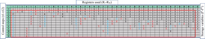
Here, storage variables (I0-I82) are designated to respective registers (R1-R42) in twelve control steps (τ1-τ12), based on dependency information.
Subsequently, in order to obtain the secure RTL datapath, scheduled and encrypted security constraints embedded CDFGs are synthesized into RTL datapath design. In order to do so, firstly, the multiplexing scheme for functional units (adders and multipliers) and storage elements (registers) is determined. The scheduled CDFG of the respective designs are exploited for the same. Post determining the multiplexing scheme, datapath and controller designs are synthesized. The synthesis process therefore produces secure RTL datapath corresponding to hardware IPs for filter bank and QRS complex of implantable cardiac pacemaker. The encrypted security constraints implanted secure RTL datapath corresponding to filter bank and QRS complex are depicted in Figs. 21 and 22 respectively, where the effect of implanting encrypted security constraints has been highlighted using red color boundary (representing change in their inter-connections corresponding to multiplexing scheme post-embedding encrypted security constraints).
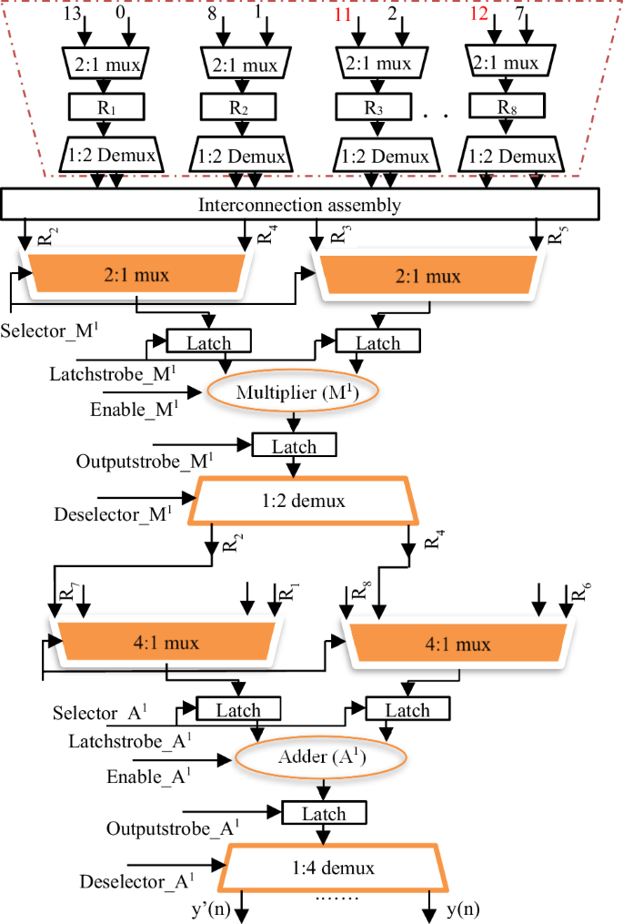
Here, the effect of implanting encrypted security constraints has been highlighted using red color boundary (representing change in their inter-connections corresponding to multiplexing scheme post-embedding encrypted security constraints).
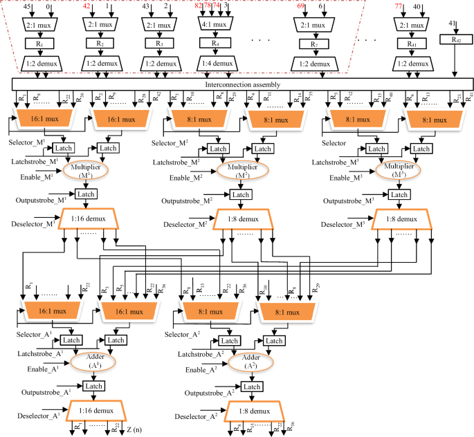
Here, the effect of implanting encrypted security constraints has been highlighted using red color boundary (representing change in their inter-connections corresponding to multiplexing scheme post-embedding encrypted security constraints).
Detection of pirated versions of cardiac pacemaker hardware IPs for end user safety
Distinguishing authentic cardiac pacemaker hardware IPs from its fake/pirated counterparts at the system integrator level, before the integration and manufacturing of the cardiac pacemaker device, is highly critical for the end safety of the patients. This is because; integration of fake/pirated cardiac pacemaker hardware IPs into a patient’s body through surgery may be catastrophic/fatal, as they do not undergo reliability and quality checks. Hardware IPs during its design process have to undergo through several stages of development, which may include untrustworthy entities (adversaries) such as an IP broker. An adversary may target to pirate the hardware IP designs without the cognizance of the authentic IP vendor. An adversary intentionally may covertly implant backdoor malicious logic into the pirated versions, which may cause fatal consequences in terms of safety hazards to the end user (patient). Therefore, in order to distinguish an authentic hardware IP from its pirated version before integration, during the piracy detection process, secret security constraints corresponding to encrypted signature of IP vendor specified strength are regenerated and matched with the information of register allocation extracted from RTL design under test. If the presence of secret security constraints corresponding to genuine IP vendor chosen signature is not found in the design, then it is probably a pirated version. However, in the proposed approach, it is extremely challenging for an adversary to precisely regenerate the covert hardware security constraints. In other words, it is extremely challenging for an adversary to bypass piracy detection process due to strong entropy (desirable) of the proposed approach. Entropy of the proposed approach is estimated in terms of the hardness of the adversarial effort in regenerating the exact signature. This is because the proposed methodology comprises of several security parameters during encrypted signature generation and implantation phases which include: (a) IP vendor specified 256 bits input signature for encryption (b) IP vendor chosen 256 bits encryption key (c) encrypted signature combination and its strength chosen by IP vendor for implanting into hardware IPs (d) IP vendor selected encoding algorithm and (e) ordering of storage variables etc. Thus, the proposed methodology, during piracy detection process, is capable to distinguish and thereby isolate the pirated versions of hardware IPs before their integration into cardiac pacemaker device. This ensures the safety of the patients carrying the implantable cardiac pacemaker.


Responses