Silicon photonics for high-speed communications and photonic signal processing
Introduction
With more than six decades of intensive research and development within the microelectronics industry, one of the most important advantages of silicon is the manufacturing infrastructure and materials processing knowledge that now enables silicon microelectronics to scale to the extremely high-yields needed in the large-volume manufacture of over 60 billion transistors per chip, all functioning flawlessly, in the mass production of microprocessors. Although a cursory glance at the optical properties of silicon, such as its indirect bandgap (inefficient light emission), centrosymmetric crystal structure (zero second-order nonlinearity for use in electro-optic (EO) modulators) shows silicon to be less suitable for discrete photonic devices than other materials, such as III–V semiconductors for lasers, or lithium niobate for optical modulators, the scalable manufacturability of silicon photonics (SiPh), enable many photonic devices to be integrated together with high yield in a photonic circuit, has propelled SiPh to become one of the mainstream technologies for photonic integration. SiPh can integrate the many different functional elements for multichannel optical transceivers and for advanced photonic signal processing applications. In this review, we focus on some of the recent advances in the technology for multichannel communications including advanced WGC for the interface of SiPh chips with optical fibers, and discuss how they can enable the efficient launch of different modes and polarization in optical fiber for high-capacity multi-lane optical communications. We also describe the SiPh based optical signal processors which can be used to unscramble the mixing of data lanes in optical fiber transmission. By implementing coherent photonic circuits which precisely control the phase of the optical signal in the circuit, we can perform matrix operations in the optical domain, and provide a low latency and power efficient alternative to the digital signal processors that have conventionally been used in high capacity optical communication systems. We also review some of the most recent advances in high-speed optical modulators in the SiPh platform. Because of space constraints, we have not included a discussion of the important advances in the heterogeneous integration of lasers with SiPh, which is discussed in other review articles1. Also, SiPh-based metasurfaces have been previously investigated2,3.
Advanced waveguide grating couplers
WGCs are fundamental functional elements, widely used device to bridge the fiber-to-chip interface. Compared with edge couplers, GCs have the advantages of arbitrary positioning on the chip surface, wafer-scale testing, relaxed fabrication and alignment tolerances, and simpler fabrication without the need for deep facet etch or facet polishing. Also, using the compact focusing design, the design layout of GCs can form two dimensional array, not easily possible with edge couplers, for interface with multicore fibers. GCs can offer sub-decibel coupling losses4,5, broad operational bandwidth6, dual polarization coupling7,8, wavelength demultiplexing9,10, perfectly vertical coupling11 for multicore fiber and multimode12 coupling for space division multiplexing. In the following section we review some of the recent advances in the technology of GCs.
High coupling efficiency silicon waveguide grating coupler
To realize high coupling efficiency (CE) of WGC, both the directionality and mode matching of the WGC should be improved. Early approaches to realize high CE grating coupler include using the apodization structure13, polysilicon overlay structure14,15, subwavelength structure with metal reflector structure16, grating with bottom Bragg reflector17, using thick waveguide layer18, dual-level grating structure19, interleaved trenches structure20 to realize high CE grating coupler.
However, most of these early approaches require a tiny feature size as small as 40 nm, possible with electron beam lithography5,21,22 but below the limitations of the 193 nm deep ultraviolet (DUV) photolithography typically used in silicon photonic foundries.
We recently proposed a new conceptual approach for the design of a high CE grating coupler with a large minimum feature size (MFS) above 180 nm which is compatible with the design rules of many commercial foundries. Unlike the previous theoretical proposal of a dual-layer grating with top and bottom etching of the silicon waveguide layer23, our proposed approach can be implemented by using a polysilicon layer deposited on the silicon grating.
The conceptual operation of the high CE grating structure is shown in Fig. 1. The optimized pattern and shifted positioning of the polysilicon overlay layer above the lower silicon grating structure makes it possible to engineer constructive interference for the upward diffracted light and destructive interference for the downward diffracted light, thus improving the directionality. A shift in position between the two layers also produces four subwavelength structures that enable a gradual change in the effective index, which can effectively provide a blazing effect of grating, and thus realize a high CE for both off-vertical angled and perfectly vertical grating couplers, as shown in Fig. 1c. The two layers combine to form subwavelength structures which enables the precise design of the grating strength of each period to further improve the mode matching and hence the overall CE.
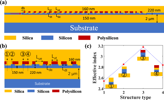
a cross-section view of the grating coupler4. b, c Four types of subwavelength structures in the vertical direction and their effective index11 (a) Reproduced with permission4 Copyright 2022, IEEE. b, c Reproduced with permission11 Copyright 2022, Optica publishing group.
In the design, the MFS is 180 nm, both the shift, period and duty cycle of each period in each layer are independently optimized using genetic numerical optimization algorithm24 to improve the CE. To reduce the simulation time, 2D FDTD simulation is used for the design optimization and 3D FDTD simulation is used to confirm the final simulation result.
To attain sub-decibel CE in the silicon WGC, we introduced a shift ds in the starting position of the polysilicon grating layer relative to the silicon grating layer in the optimization, see Fig. 1a. The initial shift is needed to provide constructive interference upwards and destructive interference downward between the upper polysilicon and the lower silicon layer, thus improving the directionality of the grating, and also helps reduce the grating strength in the first few periods of the grating to improve mode-matching with the fiber mode.
The simulation of the optimized grating coupler shows −0.68 dB CE at 1550.5 nm and 1 dB bandwidth of 33 nm. The design was fabricated, and the peak CE was measured as −0.89 dB at 1553.4 nm with 1 dB optical bandwidth of 34.8 nm (1537.6 nm to 1572.4 nm), as shown in Fig. 2.
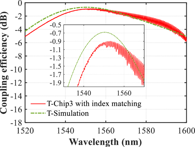
Simulation and experiment result of the sub-decibel high-efficiency silicon waveguide GC4 Reproduced with permission4 Copyright 2022, IEEE.
Table 1 compares these recent results with previously reported high-efficiency grating coupler designs. The main advance is that the sub-decibel efficiency to standard single mode fiber (SSMF) was achieved using a more robust design with a MFS above 170 nm, that was fabricated by 193 nm DUV photolithography.
Instead of the high CE, fabrication tolerance is also important in manufacturability. Figure 3 shows the fabrication tolerance of the shifted polysilicon overlay GC under different fabrication variations.
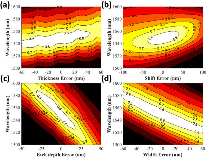
a Thickness tolerance. b Shift tolerance. c Etch depth tolerance. d Etch width tolerance4 Reproduced with permission4 Copyright 2022, IEEE.
It can be seen from Fig. 3 that the CE of the GC remains above 80% (−0.969 dB) CE for thickness error variations of −60 nm to +43 nm, shift error variations of ±40 nm, etch depth variation of −30 nm to +18 nm and etch width variations of ±60 nm. The numerical analysis in Fig. 3 shows that the high efficiency GC has excellent fabrication tolerance, and the design is suitable for large volume production. The simulated tolerance of the performance of the proposed GCs (Fig. 3) is consistent with the measured performance among different chips4,6,11 fabricated by the foundry.
Dual polarization waveguide grating coupler
The TE and TM mode in the silicon waveguide have a significant difference in effective refractive index, causing different center wavelengths for a given grating period for the TE and TM modes. Most GCs are designed to operate with only one polarization, either TE mode or TM mode. Polarization-independent GCs that can couple a randomly polarized input in the optical fiber with the PIC are needed for optical receivers and they can also enable the use of polarization division multiplexing (PDM). Typical methods to realize polarization-independent GCs include 1D GC with single port25,26, 1D GC with dual port27, and 2D GC28,29.
Recently, we demonstrated a high-performance 1D GC that can couple both TE and TM modes into a single waveguide. The conceptual operation of the polarization independent GC is shown in Fig. 4: The structure here can be regarded as a composite grating with two different gratings.
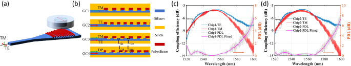
a 3D view of the perfectly vertical coupling polarization independent GC. b 2D cross-section view of the proposed GC. c, d Experiment results for the proposed polarization independent GC7 Reproduced with permission7 Copyright 2022, Optica publishing group.
Polarization independence was achieved by initially setting the periods of GC1 and GC2 for operation with TM (GC1) and TE (GC2), respectively. Then combining the two designs together, the upper polysilicon layer has the same period as GC1 for TM polarization, and the lower silicon grating layer has the same period as GC2 for TE polarization. This composite grating, GC3, can work for both TE and TM polarizations but has a relatively low CE. Using GC3 as an optimization start point, further optimization of each period/duty cycle to improve both the CE and polarization independence and get the final optimized composite grating GC4 suitable for dual polarizations (DP). The simulations predicted −3.6 dB and −3.5 dB coupling losses for the TE and TM polarization, while the perfectly vertical GC measurements had CE of −3.96 dB for TE polarization and −3.93 dB for TM polarization.
Instead of the single port 1D GC for dual polarization, dual port GCs can also be used to realize dual polarization coupling. One port is for TE polarization, and another port is for TM polarization as has been proposed27 and experimentally demonstrated30. Early designs require electron-beam lithography (EBL) fabrication and a bottom metal reflector to improve the CE to −3.8 dB. However, our recent innovation using the polysilicon overlay builds upon the previous theory27 to realize the dual port coupling of two different polarizations into two opposite directions (see Fig. 5), and the engineering of optimized shift-pattern polysilicon overlay yielded much higher CEs11,12. The schematic of the dual polarization GC is shown in Fig. 5a. The device can couple the orthogonal polarizations into two opposite directions with predicted coupling efficiencies of −1.46 dB and −1.88 dB for the TE and TM polarization and MFS of 181 nm.
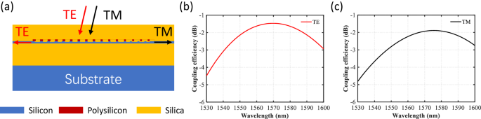
a cross-section view of the dual polarization GC. b, c Simulated CE for the TE and TM mode8 Reproduced with permission8 Copyright 2022, IEEE.
Compared with the 1D single port and dual port dual polarization GC, two-dimensional GC can couple the orthogonal modes in the fiber to the same single polarization in two silicon waveguides and avoid the use of polarization rotation devices. 2D polarization-diversity GCs have been proposed and demonstrated by many groups28,29,31,32,33,34,35,36. However, the devices fabricated by DUV photolithography in commercial foundry typically had relatively high coupling loss of 6 dB when manufactured with MFS above 180 nm37. We recently introduced a novel design for a perfectly-vertical polarization diversity two-dimensional WGC with high efficiency and low polarization-dependent loss (PDL). The basic approach used for dual polarization coupling (see Fig. 6) is based on combining the polarization diversity two-dimensional WGC28 with the optimized shift pattern polysilicon overlay method to realize high CE4 and implementing a perfectly vertical coupling11 design for a high efficiency dual polarization WGC with low PDL. This approach led to a 2D polarization diversity GC with coupling loss of 2.61 dB and theoretically zero PDL when fabricated with MFS of 171 nm38.
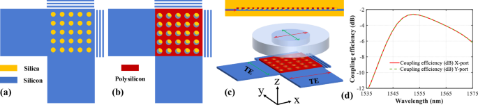
Schematic view in the (a) lower silicon layer and (b) upper polysilicon layer. c Cross-section view and schematic of the proposed two-dimensional perfectly vertical coupled dual polarization GC. d 3D simulation result for the dual polarization. Reproduced with permission38 Copyright 2024, IEEE.
Wideband waveguide grating coupler
The coupling bandwidth of GC is very narrow, typically around 1 dB bandwidth of 30 nm. Such a narrow bandwidth seriously limits the application of the GC for coarse wavelength division multiplexed (CWDM) communications. Wideband GC designs can relax the fabrication tolerances and improve the stability of coupling over a wide range of operational temperatures. Previous attempts to improve the bandwidth of the GC include reducing the index of the grating region using subwavelength structure39,40 using low index material platform19,41 using a bidirectional vertical GC42,43 using high NA optical fibers44 or using the inverse design method45,46,47 Although there are so many approaches in improving the bandwidth of GC, the bandwidth of GC fabricated by 193 nm DUV photolithography in commercial foundry was typically quite narrow, with 1 dB bandwidth of about 30 nm. We recently introduced a highly effective new design approach for wideband GCs. The new approach improves significantly on the 30 nm 1 dB bandwidth to GC with 108 nm 1 dB bandwidth. This new approach was based on the Resonant-cavity-enhanced structure, which has been previously explored for high quantum efficiency photodetector48 broadband photodetector49 and high CE GC50 We used this structure here to design wideband GC. Our proposed wideband GC has mirror symmetry about the center, as shown in Fig. 7.
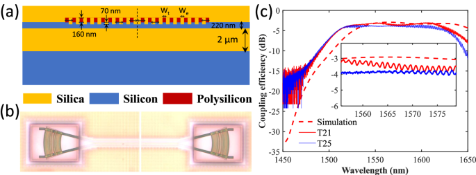
a Cross-section view and b Microscope image of the wideband GC. c Simulated and experiment result of the wideband GC6.
The structure can be regarded as the combination of many cavities around the center of symmetry. High CE is attained in a similar manner to the critical coupling concept50 in which the cavities trap light and only allow out-of-plane first-order diffraction to be the main pathway for light to escape the cavity. The diffraction mode profile is optimized to match the fiber mode to improve CE. The cavity shortens the effective length of grating by the double pass effect50 thus increasing the optical bandwidth which scales inversely with the number of periods in a grating. Also, with careful design, different cavities can be designed to have slightly different resonant wavelengths to further improve the overall bandwidth. By engineering the coupling strength between different cavities, a flat broad pass band can be realized51 and further improved by optimization of the intercoupling strength52 We can also design the structure53 to compensate for the waveguide dispersion and thus reduce the whole dispersion of the grating, and realize a broadband or colorless structure that facilitates wideband operation49
This new approach for the design of wideband GC was confirmed by both simulations and experimental measurements. The 3D FDTD simulations of the numerically optimized grating predict a CE of −2.91 dB with a 1-dB bandwidth of 109 nm, while the proof-of-concept experimental demonstration achieved an experimentally measured CE of −3.0 dB with 1-dB bandwidth of 108 nm (Fig. 7). These results show that state-of-the-art GCs for SSMF can be used in CWDM communications.
Grating couplers for MDM fiber transmission
Space-division multiplexing (SDM) uses parallel data lanes, separated spatially in different spatial or polarization modes or different fiber cores, to improve transmission capacity and interconnect density. Recent advances have resulted in MWGC which can selectively launch the fundamental (TE0) and first-order (TE1) modes from a multimode silicon waveguide to the LP01 and LP11 modes of a few mode fiber (FMF) respectively, thus providing a technology for SiPh transmitters to launch MDM channels into optical fibers.
Figure 8 shows an example of the advanced MWGC which uses the polysilicon overlay. In this example, the initial designs of the upper and lower gratings have the same period and 0.5 duty cycle. We define the normalized offset (d/(fLambda )) as negative (positive) for the upper layer left-shifted (right-shifted) with respect to the lower layer. As illustrated in Fig. 8c, zero offset results in the largest refractive index difference between the high and low index region of the grating and hence has the largest grating strength13 When the normalized offset equals −1 or +1, the resultant overall structure has the smallest index contrast and hence the smallest grating strength. By varying the normalized offsets from −1 or 1 to 0, the grating strength can be precisely engineered to apodize the grating for mode-matching with the fiber mode13 and improve CE. In addition to the shift, both the periods and duty cycles of the upper and lower layers can be numerically optimized to further improve CE.
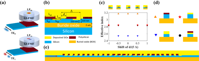
a Schematic of the high efficiency MWGC for few-mode fibers. b Cross-section view of the optimized shift pattern overlay MWGC. c The effective index of the grating subwavelength structures versus the shift of the upper polysilicon overlay layer to the lower layer grating. d The subwavelength structures produced by the shift of upper polysilicon overlay layer to the lower layer. e Cross-section of the final optimized high CE MWGC12.
Mode excitation of the LP01 and LP11 modes in the optical fiber by a single multimode grating is schematically depicted in Fig. 8a using multimode waveguide width of 15 μm. A peak CE of −1.36 dB at 1550.3 nm with 1-dB bandwidth of 34 nm for LP01 mode was experimentally measured12 The LP11 mode peak CE was −2.21 dB at 1544.1 nm with 1-dB bandwidth of 32 nm (Fig. 9). The MGC was fabricated in a commercial foundry, and had a MFS of 181 nm.
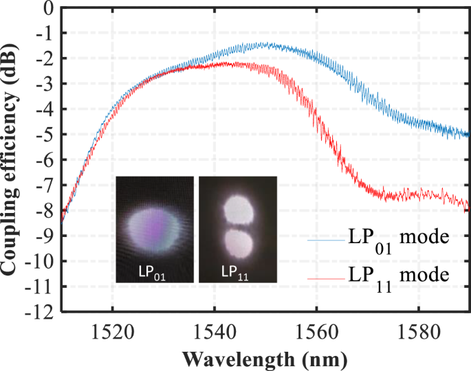
Experimentally measured CEs of the high CE multimode GC for LP01 and LP11 mode. The inset shows the excited mode field profiles of the LP01 and LP11 modes in the FMF captured by an infrared camera12.
Although this design was for a specific FMF, the same design approach could be applied for industry standard multimode fibers, such as OM4 and OM5 fiber. The OM4 fiber can support more modes which introduce challenges that require further research to solve the practical problem of how to recover some of the power scattered into the higher-order fiber modes.
It is possible to design a MWGC to selectively and simultaneously launch the TE0, TE1, and TE3 modes of the silicon waveguide into the LP01, LP11, and LP12 modes of the OM4 multimode fiber. The graded index OM4 fiber has a core diameter of 50 μm. The mode profiles of the silicon waveguide modes and the fiber modes are schematically depicted in Fig. 10b.
a Mode groups in the standard multimode OM4 fiber. b OM4 fiber modes for mode multiplexing and the corresponding silicon waveguide mode24.
The efficient coupling of three TE modes via the same MWGC is possible because their effective refractive indices in the MWGC region (which is over 30 μm in width), are very similar, leading to the same physical grating period. One can use the optimized shift pattern polysilicon overlay design approach12 to arrive at a design for a high CE MWGC that can launch the different modes into the standard multimode OM4 fiber. 3D FDTD simulations yielded the coupling efficiencies for the LP01, LP11, and LP12 modes shown in Fig. 11 of −1.95 dB for LP01 mode, −1.97 dB for LP11 mode, and −2.35 dB for LP12 mode (all with 3 dB bandwidth of 43 nm).
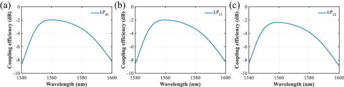
Coupling efficiency spectra for (a) LP01 mode, (b) LP11 mode, and (c) LP12 mode.
Optical signal processors for optical communications
The development of photonic signal processors based on bulk optics can be traced back to the 1960s, and numerous technologies were introduced in the 20th century54. In the 21st century, the development of integrated optics-based optical signal processors have found applications in optical communications55, optical computation56, and optical sensing57. Optical signal processors carry out the data processing in the optical domain, offering significant advantages in speed and energy efficiency over conventional microelectronic based digital signal processors58. The optical signal processors in communication systems can enhance data transmission rates and bandwidth while reducing latency58. Their high-speed signal optical processing capabilities can also be used for computing, sensing, and medical diagnostics, showcasing the versatility and potential of photonic technologies. Here we focus our review on integrated optical signal processors which are important for optical communications.
Optical signal processors for matrix processing
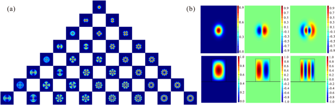
Optical signal processors can perform matrix operations in the optical domain, which is a capability at the core of advanced optical communications and high performance computing. In 1994, Reck et al. established that any discrete, finite-dimensional unitary operator could be physically realized with optical devices (Fig. 12g). They demonstrated that an N × N unitary matrix could be deconstructed into a sequence of two-dimensional transformations facilitated by beam splitters. This groundbreaking work was followed by subsequent innovations in the field59 by Clement et al. (Fig. 12f), who introduced an enhanced design for universal multiport interferometers. Their approach leverages an alternative configuration of beam splitters and phase shifters (PS), achieving a design that not only halves the optical depth compared to Reck’s original proposal but is more robust to optical losses. In both59,60 the optical processor element is the Mach–Zehnder interferometer (MZI) (Fig. 12a), which has two PS. One PS can tune the splitting ratio, while the other PS can tune the relative phase difference at the two output waveguides57 Alternative designs, such as MZIs with balanced phase shifters61 (Fig. 12b), thermally actuated Dual-Drive Directional Couplers on silicon nitride platforms62 (Fig. 12c), offer compact and low-loss solutions. In 2021, we proposed the use of the coherent four port microring resonator (MRR) as an alternative to the conventional MZI for unitary conversion63 (Fig. 12d). The basic advantage of the MRR over the MZI network comes from its more compact size and better power efficiency in tuning the MRR. The MRR-based programmable units not only can be used for unitary conversion64 but also offer advantages for applications requiring recursion, such as optical delay lines and pulse shaping. Additionally, the exploration of slow-light-enhanced periodic bimodal waveguides as programmable units has introduced a paradigm shift65 (Fig. 12e). This study experimentally demonstrates low-loss short tuning elements of 30 × 1.7 µm2 in area, achieving a two-orders magnitude integration density improvement compared to conventional MZIs. Tang et al. 66 introduced a novel, integrated, reconfigurable unitary optical mode converter(Fig. 12h). Utilizing cascaded multimode interference couplers and phase shifter arrays, it was possible to mitigate path-dependent loss and reduce the overall footprint of optical converters in photonic integrated circuits. These advances in optical signal processing technology illustrate the ongoing journey towards more efficient, compact, and robust optical devices for signal processing.
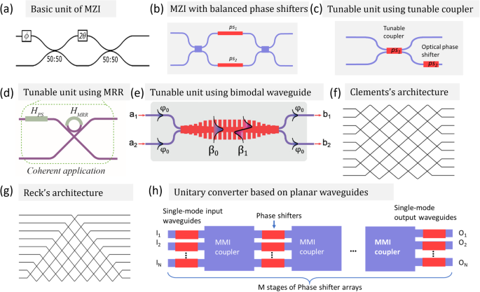
a Typical MZI. b MZI with balanced phase shifters. c Tunable directional coupler as variable beam splitter. d Micro-ring resonator-based units for unitary conversion. e Tunable units using bimodal slow-light waveguide. f, g General architecture for unitary conversion using basic units in (a)–(e). h Unitary conversion using multi-plane light conversion. a, f, and g Reproduced with permission59 Copyright 2016, Optica Publishing Group. d Reproduced with permission63 Copyright 2023, De Gruyter. e Reproduced with permission65 Copyright 2023, Wiley-VCH GmbH.
Optical signal processors for generating multimode optical fields
In 2020, Miller provided theoretical frameworks, including explicit algorithms and formulas, for calibrating optical signal processors to generate arbitrary multimode fields. This development laid the groundwork for precise control of optical signals67 (Fig. 13a). In 2023, Johannes et al. experimentally demonstrated the capabilities of a multipurpose, programmable integrated photonic processor. This processor can generate and control a different high-order free-space structured light beams using a single injection waveguide68 (Fig. 13b). Furthermore, the processor can detect the amplitude and phase distributions of structured higher-order light beams69 showing its versatility in applications. In 2023, we also demonstrated the application of MZI arrays as optical signal processors for the dynamic control of mode field distribution at the distal end of a multi-mode fiber64 (Fig. 13c). By implementing an integrated mesh of MZIs at the transmitter, we achieved controlled manipulation of the distal end mode field distribution. This is part of the technology needed to ensure low coupling losses at the receiver’s MWGC in future MDM communication systems. The use of a finite number of modes to describe, generate, and detect optical fields has proven to be both mathematically efficient and physically meaningful. Employing such a modal basis directly supports a wide range of applications in communications, sensing, and processing, illustrating the broad impact of these technological advancements.
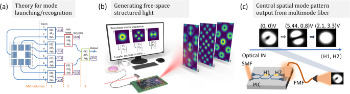
a Theoretical illustration. b Photonic processor used to generate and control free-space structured light beams. c Photonic processor used to dynamically control of the mode field distribution at the distal end of the multi-mode fiber. a Reproduced with permission67 Copyright 2020, Optica publishing group. b Reproduced with permission68 Copyright 2023, Nature. c Reproduced with permission64 Copyright 2023, IEEE.
Optical signal processors for mode unscrambling
In a typical MDM fiber communication system, the mode channels may experience mixing which introduces crosstalk to the data lanes because of mode coupling introduced by the optical fiber transmission, including the misalignment of optical fiber connectors, and physical perturbations of the optical fiber64. Previous demonstrations of MDM in multimode fiber employed digital signal processing with coherent optical communications to recover the complex amplitudes of optical fields and mitigate crosstalk effects70. However, integrated optical signal processors can perform matrix multiplication in the optical domain. These processors offer a promising alternative approach for crosstalk mitigation without the need for optical-to-electrical conversion and provide a power-efficient and low-latency crosstalk unscrambling. Optical signal processors can be broadly classified into three categories based on their applications including optical signal processors for PDM71,72, SDM73,74,75,76,77, and Wavelength division multiplexing (WDM). Specifically, in ref. 72, an all-in-one chip-scale polarization processor based on a linear MZI optical network was proposed and demonstrated as the polarization unscrambler (Fig. 14a). Additionally, MZI-based processors can be integrated with array waveguide gratings to facilitate mode unscrambling across various wavelengths simultaneously78 (Fig. 14b). Except for the linear MZI network, other types of matrix computation units have also been investigated. For example, the MRR weight banks with photonic blind source separation algorithm can be used to undo modal crosstalk in a short-reach multimode optical fiber interconnect for intra-data-center communications73. We experimentally demonstrated the utility of MRR-based networks as unitary converters for polarized mode unscrambling71 (Fig. 14c). The demonstration of an all-optical Multiple-Input Multiple-Output demultiplexing of a 300 Gbps 3-mode DP Quadrature Phase-Shift Keying signal across 1540, 1550, and 1560-nm wavelengths, utilizing the multi-plane light conversion scheme was reported to have a low energy consumption of ~1.5 pJ/bit76 (Fig. 14f). Tunable MZI mesh-based photonic processors have also been used for free-space communications. They can perform singular value decomposition and optimize bidirectional orthogonal communication channels, even for complex scattering transmission media. This approach was demonstrated to reduce crosstalk by more than 30 dB, and can be used for efficient, adaptable multimode optical communication systems75. In Ref. 77, we proposed the use of the multimode GC with the MZI arrays to compensate for the arbitrary mode crosstalk between different spatial channels at the receiver (Fig. 14 e). In ref. 79, we showed the advantage of having the optical signal processor at both the transmitter and receiver side as it enables optical singular value decomposition of the crosstalk matrix M without adding loss to the optical fiber link, while establishing the communication channels using different spatial modes (Fig. 14g). Moreover, the system-on-chip processor also has may un-mixing RF interference in real-time, enabling rapid unscrambling of received signals and recovering the un-mixed signal in under 15 ps80 (Fig. 14d). These advances show how optical signal processing can be used to unscramble crosstalk, marking a significant step towards more energy efficient and lower latency optical communication systems.
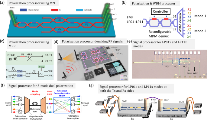
a Polarization processing using MZIs for polarization unscrambling. b Photonic signal processor for unscrambling the polarization mode crosstalk at different wavelengths. c Polarization processor using MRR for mode unscrambling. d A microwave photonic processor solves dynamic RF interference in real-time. e A receiver for unscrambling the crosstalk between LP01x and LP11x modes. f A signal processor for 3-LP dual polarization modes unscrambling. g A transceiver system using LP01x and LP11x modes with optical signal processor at both the Tx and Rx sides. a Reproduced with permission72 Copyright 2019, Nanophotonics publishing group. c Reproduced with permission63 Copyright 2023, De Gruyter. d Reproduced with permission80 Copyright 2024, ls a publishing group. e Reproduced with permission77 Copyright 2024, IEEE. f Reproduced with permission76 Copyright 2023, IEEE. g Reproduced with permission79. Copyright 2024, IEEE.
Silicon photonic modulators for high-speed communications
Optical modulator is a fundamental building block for optical transmitters81. One way to achieve high-speed modulation is by integrating thin film Lithium Niobate with a strong Pockels effect82,83. However in this review, we focus on modulator technologies that are compatible with SiPh foundries for high volume production and multichannel integration on a single chip84,85,86.
In general, modulators change the phase or intensity of incoming light to achieve modulation. Conventional Mach-Zehnder modulators (MZM) as shown in Fig. 15, modulate the phase of the incoming light, and use the interference of the MZI structure to produce intensity modulation. In data centers, non-return-to-zero (NRZ) and 4-level pulse amplitude modulation (PAM-4) formats are used for intensity modulation-direct detection (IM-DD) receivers. For longer-range telecommunication systems, coherent modulation formats, including quadrature amplitude modulation of different orders are commonly used, requiring both phase and intensity modulation, which can be implemented in an integrated MZI structure with two modulators, with 90° phase difference on one of the arms, so that I and Q channels are in quadrature. An example of such a structure is shown in Fig. 16, which uses microring modulators (MRM) in each arm of the MZI.
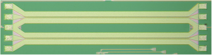
A 2500 µm length silicon photonic traveling-wave MZM.
MRM-based silicon photonic IQ modulator consists of two symmetrical arms for coherent modulation formats.
MZM, MRM, and electro-absorption modulators (EAM) are the modulators that are the widely available from different SiPh foundries87 Both the MZM and MRM, in SiPh rely on modulating the free carrier concentration in the silicon waveguide in depletion mode pn diodes while MZM offers low-frequency chirp and high extinction ratio modulation.
With the rapid rise in data center traffic, future optical transceivers will need to handle more channels, and integrate many modulators on a single chip. The relatively large footprint of MZMs is one of their major disadvantages. Another challenge of MZMs is their relatively poor energy efficiency: MZM’s typically require traveling wave electrodes that use termination resistors, resulting in high energy per bit (Ebit) of ~200 fJ/bit81. MZM typically have an inverse dependence of modulation voltage Vπ, with modulator length: it is possible to engineer long modulators with lower Vπ, but at the cost of having a larger footprint. With the traveling-wave (TW) electrode design of MZMs, there is also a limit on the maximum length of the phase shifters in each arm of the MZM determined by the electrodes’ microwave losses and the phase mismatch between the microwave electrical and optical signals. It is therefore difficult to obtain MZM with both high modulation bandwidth and low Vπ. State-of-the-art silicon MZMs have been reported with 3-dB EO bandwidth of ~47 GHz for O-band and ~46 GHz in C-band88,89, obtaining a good trade-off of between bandwidth and modulation voltage. Since the MZM modulation bandwidth typically has a slow roll-off beyond the 3-dB point, the 6-dB bandwidth is increasingly common used as a figure of merit to indicate useful bandwidth of MZM90. MZM has historically been the dominant type of modulators in optical communications systems, but the need for smaller and more energy efficient modulators has led to the increasing use of other types of modulators.
The MRM enjoys the advantages of smaller footprint, with typical ring radii ranging from 5 µm to 10 µm, and resonance enhancement which can reduce the required modulation voltage. The microring cavity has periodic resonances, and it is typically necessary for the MRM to operate with electrical heaters that lock the resonances to match the wavelength of the laser91,92,93,94,95,96,97,98. With their smaller device size, the MRM has smaller PN junction capacitance, allowing them to have much wider intrinsic RC bandwidth than MZM. The wavelength dependence of MRM makes them suitable for selective modulation of a particular wavelength in WDM communications. The MRM bandwidth is typically limited by RC time constant and the photon lifetime. The RC time constant is determined by the PN diode and contact pads, while the photon lifetime depends on the quality factor (Q) of the resonator. In general, small radii MRMs can achieve a larger bandwidth because of the reduced device capacitance and shorter photon lifetime (Fig. 17).
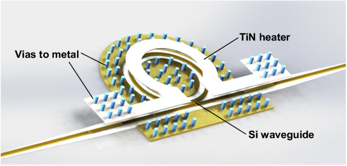
Overview structure of an MRM showing waveguides, heater and vias for metal connection. Reproduced with permission91. Copyright 2022, Optica Publishing Group.
GeSi-EAM, utilizing the Franz-Keldysh (FK) effect within the SiPh platform, is another alternative for silicon photonic modulators85,99,100. Ge-Si EAM offers advantages such as high bandwidth, a compact size, low driving voltage, and an effective optical bandwidth of 30 nm within the C-band without needing the thermal heater control that MRM requires. The low driving voltage of EAM and their low device capacitance contribute to high energy efficiency, which has been reported to be as low as 9.0 fJ/bit (NRZ)100. Compared to conventional carrier-depletion MZMs, GeSi-EAM demonstrates good potential for energy-efficient modulation and small size for integration of many modulators on a single chip.
State-of-the-Art Silicon photonic modulators
Recent advances in SiPh modulators have pushed the modulator performances close to the practical limit set by physical dimensions and the free carrier mobility of silicon. In high-performance MZMs, demonstrations have shown the capability of MZMs to operate beyond its 3 or 6-dB bandwidth, achieving high baud rate transmissions at over 100 Gbaud and net bit rates over 300 Gb/s90. To lower the driving voltage of conventional MZMs and potentially raise the bandwidth of the modulator, segmentated MZMs were proposed, which features multiple MZM connected in series. Each segment serves to modulate 1 bit, which for PAM-4, would require two segments. This design can achieve lower driving voltages and have a higher modulation bandwidth. However, it requires segments to be electrically phase matched to achieve a good signal quality. This raises the driving requirement and needs specific tuning to match the electrical phase driving the different segments and each segment requires a separate modulator driver.
MRMs have been achieving state-of-the-art results in terms of data rate, and more importantly, the modulation area density, which is enabled by its ultra small device size. In our recent demonstrations, we employed a MRM with PAM-8 and PAM-4 data modulation formats to achieve 330 Gb/s (110 GBaud) with PAM-8 and 280 Gb/s (140 Gbaud) using PAM-497. The device was fabricated in a multi-project wafer at a commercial foundry. To achieve PAM-8 using MRM, the modulator design needs to be optimized for efficiency. With the ring radius of 7.5 μm, we obtained a MRM with over 50 GHz EO bandwidth and Vπ·L of 0.63 V·cm. The design allowed for PAM-8 modulation under typical driving voltages that can be provided by commercial modulator drivers at 100 Gbaud. Our demonstration on MRM extended the data rate record of silicon MRM for both PAM-4 and PAM-8 modulation (Fig. 18).
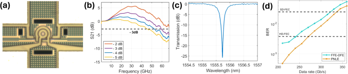
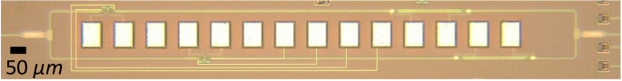
330 Gb/s MRM. a Fabricated device, b EO S21, c optical transmission, d PAM-8 BER (EO: electro-optic.). Reproduced with permission97. Copyright 2023, Optica Publishing Group.
With the MRM being a great candidate for WDM systems, there remains potential to further improve their design to provide better uniformity across wavelengths. This can allow for the use of a single modulator design for a complete WDM system, which can greatly save time on device design and optimization since only one design is needed instead of multiple designs for different wavelengths.
While conventional MRM can achieve excellent performances as shown above, also with its wavelength selectivity favoring its use for WDM applications, conventional MRM designs face a drawback when used at wavelengths outside their nominal designed wavelengths, where the extinction ratio can have variations, causing a drop in performance. Fig 19 shows our recent design of an ultra-wide operation wavelength range MRM which uses an adiabatic microring modulator (AMRM)101. By utilizing an adiabatic waveguide design, the coupling ratio is kept within 0.5 dB variation across a 100 nm simulated range, resulting in the fabricated AMRM having an operation wavelength range of over 80 nm with an extinction of over 20 dB across the entire range. The AMRM also has a high 3-dB EO bandwidth of over 60 GHz. With the AMRM, we achieved PAM-4 modulation up to 125 Gbaud (250 Gb/s). With the modulator’s ultra compact footprint of 20 μm x 20 μm, the wide operation wavelength range and the wavelength selectivity the same as MRM, it is suitable for realizing large channel count transceivers utilizing WDM in future data center interconnects.
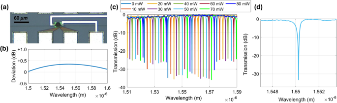
a Device photograph, b coupler transmission deviation (simulated), c measured device spectrum under different heater power, d measured device transmission with resonance at 1550.25 nm. Reproduced with permission101. Copyright 2024, Optica Publishing Group.
GeSi-EAM offers the advantages of simpler control and small footprint. By integrating GeSi-EAM and GeSi-photodiode in a transceiver for IM-DD within the C-band, we achieved the first operation of a single GeSi-EAM with a GeSi-PD at 112 Gbaud100. PAM-4 modulation was demonstrated at various data rates (168 Gb/s to 240 Gb/s) using the modulator (Fig. 20). The integrated photodiode had 3-dB bandwidth exceeding 65 GHz and a responsivity of 0.8 A/W at 1550 nm. Linear feed-forward equalization (FFE) and decision feedback equalization (DFE), along with an optimized FFE-DFE-based third-order polynomial nonlinear equalizer, were employed in a 100Gbaud+ system operating in the C-band. We successfully showcased an integrated transceiver designed for optical interconnects, operating at baud rates of 112 Gbaud (224 Gb/s), 108 Gbaud (216 Gb/s), and 100 Gbaud (200 Gb/s) in back-to-back (B2B), 1 km, and 1.5 km SSMF transmissions, respectively. The state-of-the-art data transmission rate of 224 Gb/s in the C-band using GeSi-EAM highlights the potential of the EAM technology for realizing high-capacity, cost-effective transceivers in future data center interconnects. We also made a comparison table of the state-of-the-art silicon modulators summarized in Table 2.
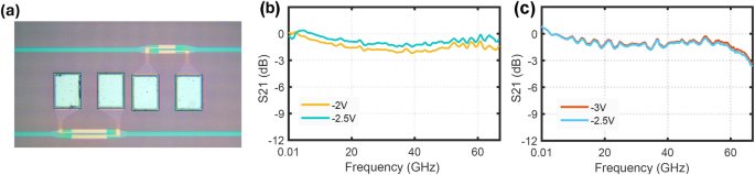
a Fabricated transceiver, b EO S21 of GeSi-EAM, c OE S21 of GeSi-PD. Reproduced with permission100. Copyright 2022, IEEE.
Discussion
In this article, we reviewed recent advances in advanced waveguide GCs, optical signal processors and high-speed modulators on the silicon photonic platform for possible future applications in high-capacity multichannel communications. The advanced waveguide GC can enable dual polarization, multiwavelength and multimode light coupling with high efficiency between the photonic integrated chip with the fiber. With the optical signal processors, the dual polarization and multimode light can be unscrambled into multichannels with low crosstalk and then modulated these multi-data channels with high-speed modulators will enable high-speed and high-capacity communications for future communication networks with silicon photonics.
Responses