Spintronic devices for biomedical applications

Introduction
Spintronic devices have attracted great research attention in the last three decades. Different from semiconductors, spintronic devices rely on the intrinsic spin of electrons to encode and process information, offering novel functionalities and improved performance compared to traditional electronic devices. Examples of spintronic devices include magnetic random-access memory (MRAM)1,2,3, spin transistors4,5,6,7, spin filters8,9,10,11, THz emitters12,13,14,15,16, and sensors17,18,19,20,21. In industry, spintronic devices play a crucial role in data storage technologies such as hard disk drives (HDDs) and solid-state drives (SSDs), offering high-speed data access and non-volatile memory capabilities22,23. Spintronic devices also contribute to the development of spin-based oscillators for precise timing in communication systems and spin-based logic devices for next-generation computing architectures, promising significant advancements in computational efficiency and performance24,25. In biomedical areas, biosensors that are based on spintronic devices have been utilized as diagnostic tools for detecting biomolecules and analyzing DNA sequences with exceptional precision26,27,28.
Among the long list of spintronic devices documented to date, giant magnetoresistance (GMR) devices, magnetic tunnel junctions (MTJ), and anisotropic magnetoresistance (AMR) devices represent the earliest generation. They have undergone extensive study and research, resulting in their maturity marked by high performance, repeatability, and robustness. Their proven reliability has led to widespread utilization in both biomedical and industrial applications. In this review, we direct our focus toward exploring the biomedical applications of GMR, MTJ, and AMR biosensors, as depicted in Fig. 1. It is worth noting that newer spintronic devices, such as spin Hall oscillators29 and spin torque oscillators30,31, have been proposed for biomedical use as well. However, owing to limited literature, inadequate experimental demonstrations, and insufficient evidence regarding their robustness and repeatability, this review does not encompass these newer spintronic devices.

Reprinted with permission from ref. 26 copyright 2022 American Chemical Society. Reprinted from ref. 90 licensed under the terms of the Creative Commons Attribution License CC BY 4.0. Reprinted from ref. 175 licensed under the terms of the Creative Commons Attribution License CC BY 4.0. Reprinted from ref. 176, licensed under the terms of the Creative Commons Attribution License CC BY 4.0. Reprinted from ref. 163, licensed under the terms of the Creative Commons Attribution License CC BY 3.0.
This review follows a logical structure outlined as follows: In Section “Giant Magnetoresistance (GMR)-based Biomedical Applications”, we start with an introduction to GMR devices and their applications in biomedicine. We cover the GMR effect, and variations of GMR structures including GMR multilayer structures, GMR spin valves, and granular GMR configurations. Additionally, we highlight the significance of flexible GMR sensor designs, particularly suitable for wearable applications. The remainder of this section is dedicated to elucidating the biomedical applications of GMR devices, focusing on their utility in bioassays, as well as in recording cardiac and neuronal signals. Section “Magnetic Tunnel Junction (MTJ)-based Biomedical Applications” examines MTJ devices and the tunneling magnetoresistance (TMR) effect, accompanied by illustrative examples of MTJ-based bioassays and recordings of cardiac and neuronal signals. While AMR effects initially found use as magnetic field sensors, their relatively low magnetoresistive (MR) ratio compared to GMR effects and MTJ has hindered widespread adoption in magnetometry and biomedical applications. In Section “Anisotropic magnetoresistance (AMR)-based Biomedical Applications”, we report the working principles of AMR-based devices and present several examples of AMR-based biosensors. In Section “Challenges and Opportunities”, we address the challenges confronting MR sensors in biomedical applications. These challenges include the rising need for enhanced detection limits, the requirement for reliable on-field testing capabilities, ensuring sensor reliability and stability in complex testing environments, managing costs, and achieving consistent repeatability of results.
Giant magnetoresistance (GMR)-based biomedical applications
GMR effect and devices
GMR effect
Giant magnetoresistance (GMR) is a quantum mechanical effect representing a remarkably intriguing innovation in thin-film magnetism with vast potential applications. The discovery of the GMR effect dates back to 1988 when Albert Fert and Peter Grünberg first observed it in (001)Fe/(001)Cr superlattices structures of interchanging ferromagnetic (FM) and nonmagnetic (NM) multilayer32. These superlattices were fabricated through molecular beam epitaxy (MBE). The evolution of thin film layer fabrication techniques, such as MBE, sputtering, and electrodeposition, has played a pivotal role in unlocking the possibilities for stacking FM and NM multilayers33. These multilayer thin film stack materials behave physically in a way entirely dissimilar from their corresponding bulk materials.
Below the Curie temperature of the FM material in the GMR device, the “giant” change of electrical resistance can be elucidated qualitatively through the Mott two-channel model depicted in Fig. 2A, B34,35. According to the Mott model, the metal layer’s electrical conductivity is contingent upon the corresponding electron spin direction and the scattering of the conduction electron. The scattering of the conduction electrons, while passing the FM layers, depends on the magnetizations of the FM layers. It can be evident from the FM/NM/FM configuration shown in Fig. 2A: i that when both FM layers are magnetized parallel, the conduction electrons with spin-up can easily pass through without scattering, indicating the low resistance path. Conversely, spin-down conduction electrons experience significant scattering because of their opposite spin directions from the magnetization direction of the FM layer, which leads to the occurrence of high resistance. This phenomenon of conduction electron scattering owing to FM layer magnetization directions is further expounded through the Density Of States (DOS)36,37,38,39 diagram in Fig. 2A: ii. The Density of States (DOS) is defined as the number of states per energy range (E), and the Fermi level (EF) determines how many energy states that are filled up by electrons (For instance, in the DOS below the EF are filled with electrons and the DOS above the EF remains unfilled). For NM material, the EF in the DOS is in a balanced position for both spin-up and spin-down, as no unbalanced spin polarization exists. However, due to the presence of unbalanced spin polarization in the FM layer, a different EF in DOS is observed for spin-up and spin-down electrons. For example, Fig. 2A: ii shows that the FM layer is magnetized in the spin-up direction; therefore, it has less unfilled space in DOS for spin-up and more unfilled space in DOS for spin-down direction. Similarly, in Fig. 2B: ii, the first FM layer is magnetized in the spin-up, and the second one is magnetized in the spin-down; therefore, more unfilled space in DOS is observed at spin-down for the first FM layer and more unfilled space in DOS for spin-up for the second FM layer, respectively. The elevated DOS above the Fermi level contributes to the high scattering of conduction electrons, leading to the high resistivity in those regions.
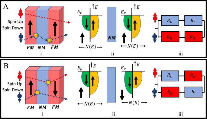
A when both FM layers magnetized in the same direction: (i) spin-dependent scattering, (ii) the schematics of DOS for the concerning magnetizations of the FM layers, whereas ({{rm{E}}}_{{rm{F}}}) is the Fermi level, N(E) is DOS, and E is electron energy, (iii) resistor model schematics where the high resistance is ({{rm{R}}}_{{rm{H}}}) and low resistance is ({{rm{R}}}_{{rm{L}}}). Similarly, in (B) when the FM layers are magnetized into antiparallel directions, (i) spin-dependent scattering, (ii) schematic for DOS, and (iii) schematic of resistor model, respectively.
Moreover, due to the minor probability of spin-flip in the metal layer scattering process, initial spin is preserved40, and it can be represented further as the two parallel resistance models in Fig. 2A: iii, B: iii. Comparable occurrences can also be noted when FM layers are magnetized antiparallel, as depicted in Fig. 2B.
The key distinctions between GMR, ordinary magnetoresistance, and anisotropic magnetoresistance (AMR) lie in their underlying mechanisms. Ordinary magnetoresistance results from Lorentz force on electrons due to the magnetic field, and the AMR originates from the spin-orbital interaction (SOI), which depends on the orientation of the electric current. Concurrently, the resistivity variation in GMR arises from the local multilayered magnetic configuration40.
GMR multilayer structure
The GMR effect is a substantial change in the resistance of multilayered structures concerning the relative magnetization directions of the FM layers, as depicted in Fig. 3A. The GMR effects in multilayered structures are obtained by an antiparallel alignment between the magnetizations of neighboring FM layers that can be achieved by the antiferromagnetic interlayer exchange coupling41, resembling the Ruderman–Kittel–Kasuya–Yosida (RKKY) interaction. Additionally, due to the distance-dependent nature of the RKKY40,42, the antiparallel configuration of FM layers can be achieved by choosing the precise thickness of the NM layer. Another possible way to achieve the GMR effect without having an antiparallel configuration is by choosing the FM layers with different coercivities43,44 as well as by manipulating the switching condition of soft and hard FM layers subject to an external magnetic field.
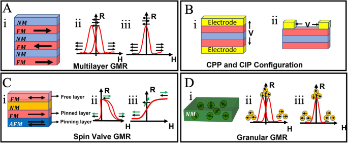
A GMR multilayer structure. B (i) CIP and (ii) CPP configuration with gold contact electrodes. C GMR spin valve structure. D Granular GMR structure. A: ii, iii), C: ii, iii, and D: ii, iii represent the R-H curves of the corresponding GMR structures.
In the absence of an external magnetic field, the FM layers are coupled antiferromagnetically, and using the external magnetic field, these FM layers can be aligned in the same direction. When the FM layers are aligned in a parallel direction, the electrical resistance of the GMR device is low (RP). On the contrary, when the FM layers are antiparallelly aligned, the resistance of the GMR device is high (RAP). Therefore, the magnetoresistance (MR) ratio of the GMR can be defined as:
The resistance change phenomena are illustrated in Fig. 3A: ii. Figure 3A: ii represents the GMR effect due to choosing FM layers with different coercivities.
Two main approaches for measuring the GMR effect are current in the plane (CIP) and current perpendicular to the plane (CPP), depicted in Fig. 3B. Since it takes a less complicated strategy than CPP, CIP is typically favored in trials between the two methods. Moreover, the low CPP resistance of the thin GMR multilayers makes them challenging to detect, and one recommended technique for these measurements involves superconducting connections for these measurements26,45. Thus, these approaches (CPP and CIP) of measuring the GMR effect depend on how the current passes through the multilayers.
GMR spin valve (SV) structure
The structure depicted in Fig. 3C represents a GMR spin valve configuration comprising two FM layers separated by the NM layer. In this arrangement, the magnetization of one FM layer adjacent to the antiferromagnetic layer (AFM layer) is pinned by the exchange coupling interaction, while the other FM layer is free to revolve around with the influence of an external magnetic field. As the AFM layer restricts the adjacent FM layer rotation, it is referred to as the pinning layer, and the adjacent FM layer is called the fixed or pinned layer (as illustrated in Fig. 3C: i).
In a spin valve configuration where the magnetizations of both ferromagnetic (FM) layers and the antiferromagnetic (AFM) layer align along the easy axis, the magnetization of the unpinned FM-free layer reverses, while that of the pinned FM layer remains unaffected. This behavior is contingent upon the transition of the applied external magnetic field from negative to positive46. This causes the resistivity to increase steeply in a minimal field range. In Fig. 3C: ii, the free layer magnetization is denoted as a green arrow, and the pinned layer magnetization is denoted as black. Similarly, in the spin valve configuration, when the magnetization of AFM (pinning layer) and FM (pinned) are annealed to the hard axis, while the magnetization of the top free FM layer remains aligned along the easy axis direction, then a linear R-H curve of Fig. 3C: iii is obtained. This is because the pinned FM layer magnetization is perpendicular to the free FM layer magnetization, and the free layer can only rotate with the applied magnetic field. The maximum resistivity is obtained when the free FM layer is antiparallel to the pinned layer. Hence, the GMR spin valve is more advantageous in comparison to the multilayer GMR structure, although the measured GMR ratios in the multilayer structures are higher than in spin valves. In GMR spin valves, low magnetic fields are sufficient to induce the structure’s resistance change, making it an attractive option as magnetometers for detecting weak magnetic fields.
Granular GMR
Even though the first GMR was observed in the multilayer FM/NM interface thin film structure, the fundamental mechanism of GMR remains elusive and, so far, proposed only phenomenological models47. In 1992, two groups, Xiao et al.47. and Berkowitz et al.48, independently reported the granular GMR in a Co-Cu alloy thin film, whereas Co magnetic nanoparticles (MNPs) are embedded inside the Cu NM conductive matrix, as shown in Fig. 3D. Due to the presence of the MNPs in the NM conductive layer, the granular GMR also exhibits spin-dependent scattering. The embedded MNPs in the NM layers directly trace the path of the applied magnetic field. Therefore, the resistance of the layer is influenced by the relative orientation of the magnetization of the MNPs, a characteristic that can be manipulated by an external magnetic field. For instance, without an external magnetic field (H = 0), the magnetizations of MNP align randomly, resulting in maximum scattering of the conduction electrons and causing the resistance to be at maximum, as shown in Fig. 3D: iii. Conversely, the minimum resistance occurs while the magnetizations in MNPs are aligned with either a positive or negative external magnetic field, as illustrated in Fig. 3D: iii. The two peak resistances are observed during the forward and backward scanning due to the presence of coercivities in the ferromagnetic MNPs. On the other hand, Fig. 3D: iii depicts the RH curve of granular GMR when the MNPs are superparamagnetic.
Much research has been carried out to explain the granular GMR properties in various conditions. For instance, Spizzo et al. demonstrated the GMR effect as a function of temperature for various concentrations of FexAg100-x granular samples49. Their work demonstrated the low-temperature effect on magnetic structures and showcased that interparticle magnetic interaction has a twofold effect on magnetoresistance. The induced correlations among the particle magnetic moments affect the GMR intensity. They concluded that GMR intensity reduces due to particle interactions and the GMR effect is enhanced at the low temperature. For Co-Ag granular structures, the authors Xiong et al. demonstrated the magnetotransport properties and the Co particle size-dependent magnetoresistance for spin-dependent scattering50. Furthermore, Meyer et al.51 utilized the carbon shell Co nanoparticles and tested out for four different types of various conductivities and viscosities gel matrices of (i) water, (ii) 2% agarose gel, (iii) conductive electrode gel, and (iv) 2:1 mixture of glycerin and water. They noted the highest MR ratio of 260% for water-based gel matrix configurations. They also found that particles in low viscosity medium can form chain fragmentations and small clusters that increase the MR ratio. Whereas, in a high-viscosity medium, particles cannot form a chain, resulting in a decreased MR ratio of only 12%. Importantly, another essential point they have experimentally demonstrated is that if the gel matrices dry up, it dramatically reduces the GMR effect because the container matrix starts to lose its conductivity and become more resistive.
The granular GMR fabrication is most commonly performed using (i) the top-down method, which involves the co-sputtering and co-evaporation of granular particles deposited into the substrate, and (ii) the bottom-up method, which involves the prefabricating particles in NM matrix material from the alloy52.
Flexible GMR sensors
GMR sensors on flexible substrates
Flexible sensors, including flexible GMR sensors, have been a focal point for research groups due to their potential for diverse in vivo and on-body applications53. The inception of flexible GMR sensor fabrication can be traced back to the 1990s54. The predominant method for creating flexible GMR sensors involves directly depositing GMR stacks onto inherently flexible polymer substrates, such as polyimide (PI)55, polyethylene terephthalate (PET)56,57, and polyethylene naphthalate (PEN)58, etc. For instance, Ferreira et al. fabricated GMR spin valve sensors by directly depositing GMR stacks onto commercially available PET and PI foils59. In Fig. 4A: i, a demonstration of flexibility is showcased through the patterned GMR spin valve sensor on a 25 μm thick PET foil. The magnetic properties of these flexible GMR sensors are assessed through both experimental measurements and simulations using a macro-spin model developed based on the Stone-Wohlfarth model. Figure 4A: ii & iii displays the experimental and calculated transfer curves of the spin valve sensors on PET and PI, respectively. These curves reveal the linear and nearly non-hysteretic transfer characteristics of the patterned GMR sensors on polymeric foils.
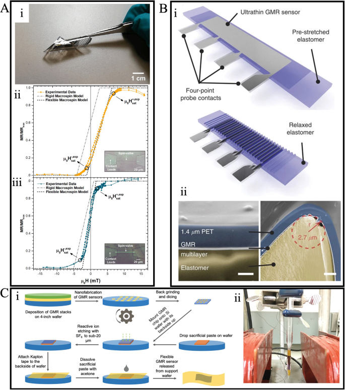
A (i) Photo of GMR sensor on flexible PET foil. (ii-iii) Transfer curves of GMR sensors on (ii)laminated PET foil, and (iii) PI foil. B (i) Schematic representation of stretchable GMR sensor. (ii) Cross-section SEM images show the detailed structure of the wrinkle. C (i) Schematics of the fabrication of flexible GMR biosensors. (ii) Flexible GMR sensor wrap on the glass tip with a radius of 1 mm. A Reprinted with permission from ref. 59, copyright 2021 Elsevier B.V. B Reprinted from ref. 61, licensed under the terms of the Creative Commons Attribution License CC BY 4.0. C Reprinted from ref. 62, licensed under the terms of the Creative Commons Attribution License CC BY 4.0.
Flexible polymeric substrates also add stretchability to GMR sensors. Achieving a highly stretchable GMR sensor often involves inducing wrinkles in the polymer substrates60. For example, Melzer et al. transferred a fabricated GMR sensor from a PET foil onto a 3 M very high bond (VHB) pre-stretched elastomer with uniaxial strain61. As depicted in Fig. 4B: i, upon the release of stress, the elastomer and the sensor layer form wrinkles, enabling stretching of the GMR sensor along the initial deformation direction. The cross-sectional SEM image in Fig. 4B: ii provides a detailed perspective of the wrinkled sensor structure. Remarkably, this stretchable sensor can maintain its GMR ratio and relative resistance even under strains of up to 270%.
In addition to inherently flexible films, substrates initially rigid can be rendered flexible by reducing their thickness. This method was employed by Su et al. to fabricate a GMR biosensor for cancer cell detection62. Illustrated in Fig. 4C: i, a GMR stack was initially deposited on a rigid silicon wafer. Post-fabrication, the sensor chip underwent flexibility enhancement through thinning to below 20 μm via back grinding followed by reactive ion etching. Subsequently, the ultra-thin flexible GMR sensor on a silicon membrane was affixed to a Kapton tape and wrapped around a glass tip with a 1 mm radius, forming a needle-type sensor, as shown in Fig. 4C: ii. The biosensing capability of this flexible needle-type GMR biosensor was demonstrated through the detection of cultured canine osteosarcoma cells (OSCA-8 cells) labeled with nickel magnetic nanowires. The sensor proved to have a detection limit of 104 cells/mL.
Printable GMR sensors
Fabricating flexible GMR sensors using conventional methods, whether through direct deposition on a flexible substrate or transforming a rigid substrate into a flexible one, is frequently a cumbersome process involving various fabrication steps. Consequently, printing methods have garnered significant research attention due to their cost-effectiveness and compatibility with flexible substrates63.
In 2012, Karnaushenko et al. pioneered the demonstration of a printable GMR sensor64. They formulated a magneto-sensitive ink by combining giant magnetoresistive flakes with a liquid polymeric binder solution. This ink was subsequently applied to diverse substrates, such as paper and polymer, indicating its adaptability to flexible substrates. To date, while the specific materials employed may vary, the fundamental methods for preparing giant magnetoresistive ink have remained consistent65,66,67. In Fig. 5A, a detailed schematic illustration depicts the process of preparing GMR ink65. This involves depositing a giant magnetoresistive multilayer stack on a rigid substrate with a sacrificial layer, followed by lifting off the giant magnetoresitive stack through the dissolution of the sacrificial layer. The resulting lifted giant magnetoresistive stacks are then ball-milled into micro-sized flakes and blended with a polymeric solution to create a printable ink. This polymeric binder solution serves to establish both electrical and structural connections among the giant magnetoresistive flakes.
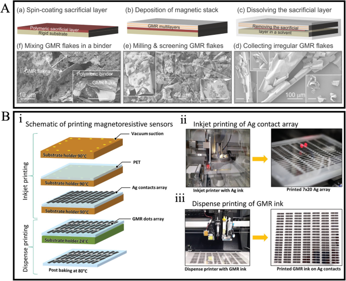
A Schematic illustrations of preparing GMR ink. (ii-iii) Transfer curves of GMR sensors on (ii) laminated PET foil and (iii) PI foil. B (i) Schematic of the printing process. (ii) Inkjet printed Ag contact. (iii) Dispense printed GMR sensor on Ag contacts. A Reprinted from ref. 65, licensed under the terms of the Creative Commons Attribution License CC BY-NC 4.0. B Reprinted from ref. 67, licensed under the terms of the Creative Commons Attribution License CC BY 4.0.
Recently, Gupta et al. achieved the large-scale manufacturing of 370 operational GMR sensors on a flexible PET foil by printing a flake/polymer composite paste67. The giant magnetoresitive flakes employed were ball-milled Co/Cu multilayers, and the polymeric binder solution was polyepichlorohydrin (PECH) dissolved in an ethyl acetate solvent. As shown in Fig. 5B, the printed sensor was prepared by inkjet printing an Ag contacts array on the PET film, followed by dispense printing of giant magnetoresistive ink on Ag contacts. With 1 mL of giant magnetoresistive ink printed on each sensor, an average GMR value of around 18% was achieved for the 370 printed GMR sensors.
In addition to using micro-sized flakes for magneto-sensitive ink, magnetic particles can be utilized as functional fillers in a binder solution to create magnetic printable sensors68,69,70,71. For instance, Kim et al. achieved various 3D shapes with programmed ferromagnetic domains via the 3D printing of NdFeB micro-particles blended with a silicone-based elastomer mixture72. Oliveros-Mata et al. developed a printable MR sensor using a non-magnetic green alternative to MNPs, namely bismuth (Bi)73. Through dispenser printing techniques, they successfully fabricated a Bi-based sensor demonstrating a room temperature MR of 146% at 5 T. While a printable GMR sensor made of MNP/polymer ink has not yet been realized, the discovery of a polymer-based granular structure51, as discussed in Section “Granular GMR”, suggests the potential feasibility of achieving an MNP-based printable GMR sensor.
Different GMR sensor shape designs
Linear response with minimal hysteresis in an external magnetic field is considered a crucial requirement in the design of any magnetic biosensors. In GMR sensors, achieving high linearity in resistance versus magnetic field curve (R-H) under a low magnetic field involves employing various approaches, such as introducing anisotropy74 and optimizing the magnetic stack designs75. Also, there is a tradeoff between the sensitivity (MR ratio) and the linearity in GMR sensors. For instance, the spin valve GMR exhibits higher linearity and can also work in the lower magnetic field compared to the multilayered GMR structure; however, they exhibit lower sensitivity as in spin valve GMR, only two FM layers contribute to the GMR effect28.
One of the most straightforward methods to enhance linearity is to design sensors with a high aspect ratio, incorporating shape anisotropy through structures such as stripes, spirals, and meanders. However, the stripe shape GMR sensors come with certain risks and drawbacks. They are prone to open circuitry, and even minor fabrication defects in the thin giant magnetoresistive layers can lead to breakage. For this reason, multiple giant magnetoresistive stripes are often connected in series and parallel configurations to address these issues. Another challenge is the limited effective sensing area due to the necessity of a high aspect ratio. This limitation reduces the number of MNPs that can be captured, especially in applications involving biological detection. In addition, for stripe-shaped GMR sensors, the signal from MNPs varies depending on their position within the stripe. It is reported that the MNPs at the edge of a GMR sensor contribute higher signals than those in the middle, and also, the magnetic signals sensed from MNPs located in the middle and the edge of a sensor can cancel out, resulting in SNR degradations76. To overcome these challenges, researchers have explored the use of large-area GMR sensors with lower aspect ratios and larger effective sensing areas77. Several recent works have focused on developing GMR sensors with larger sensing areas. For instance, Su et al. demonstrated that the signal obtained from a larger area GMR sensor is approximately 20 times greater than that from stripe sensors when detecting MNPs at concentrations of 50 MNPs/µm2 78. They highlighted the sensitivity limitations of stripe-shaped sensors by detecting immunoglobulin G (IgG) protein and emphasized the advantages of larger GMR sensors, including the role of reverse nucleation sites in magnetization switching. Thus, fabricating GMR spin valve sensors with a larger area is more straightforward than stripe-shaped GMR sensors.
GMR-based bioassays
An important biomedical application of GMR sensors is detecting biomolecules. The general detection principle of GMR-based biosensors involves labeling target analytes with magnetic labels (e.g., MNPs or magnetic beads) and detecting the stray fields generated by these labels. (Authors’ note, for convenience, we collectively call these magnetic labels ‘MNPs’ in this review.) Utilizing MNPs as labels gives the GMR-based biosensor an advantage over counterparts like optical and chemical sensors due to its inherently low background noise, given the non-magnetic nature of most biological samples. Since the stray fields generated by MNPs decay rapidly with distance, establishing bioassays on the sensor surface is crucial to bringing MNPs in proximity for the stray field to become detectable. Additionally, these bioassays establish a quantitative relationship between MNPs and target analytes, ensuring accurate detection.
Depending on the nature of the target analytes, the GMR-based bioassay can take the form of either a protein-based immunoassay or a DNA-based assay. GMR-based immunoassays have shown efficacy in disease diagnosis79,80,81,82, foodborne pathogen detection83,84,85, and allergen detection86. For example, Sun et al. established a GMR-based sandwich immunoassay for detecting prostate-specific antigen (PSA)81, as illustrated in Fig. 6A: i. The sandwich assay structure involves a capture antibody/target analytes/detection antibody configuration. This type of immunoassay is widely used in GMR-based biosensing systems for its high detection specificity. Notably, their approach differed from many GMR-based biosensors, as they built the immunoassay on a separate glass surface rather than directly on the sensor surface. During testing, the immunoassay-decorated glass slides are placed face down onto the GMR-based biosensor, as depicted in Fig. 6A: ii. This contactless detection method enhances the reusability of the GMR-based biosensor.
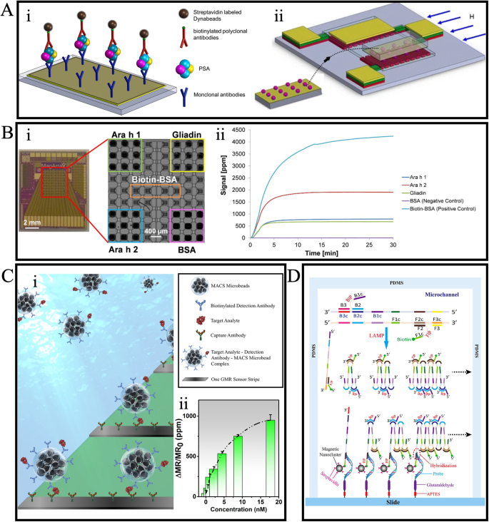
A Schematic illustrations of the (i) sandwich immunoassay and (ii) separation detection mechanism. B (i) GMR chip contains an 8 × 10 sensor array. (ii) Real-time response curve of multiplexed detection of three allergens, BSA, and biotin-BSA. C (i) Schematics of wash-free sandwich bioassay on the GMR sensor. (ii) Averaged signal recorded during the detection of IAV nucleoprotein across varying concentrations. D Schematic drawing of the genotyping process in the microchannel. A Reprinted with permission from ref. 81, copyright 2016 Springer Science Business Media New York. B Reprinted with permission from ref. 86, copyright 2016 Elsevier B.V. C reprinted from ref. 90, licensed under the terms of the Creative Commons Attribution License CC BY 4.0. D Reprinted with permission from ref. 94, copyright 2013 Elsevier B.V.
Besides single analyte detection, achieving multiplexing detection is possible if different capture probes (e.g., capture antibody, capture DNA, etc.) are decorated on individual GMR sensors on a single chip. The strong distance dependence of stray fields generated by MNPs makes it unlikely for the stray field from MNPs bound to one GMR sensor to affect others, facilitating easy multiplex detection. For instance, Ng et al. demonstrated multiplex detection of three types of food allergens on a giant magnetoresistive chip with an 8 × 10 sensor array86. Capture antibodies for two major peanut allergens, Ara h 1 and Ara h 2, as well as the wheat allergen Gliadin, were each functionalized on nine sensors within the sensor array, as shown in Fig. 6B: i. Subsequently, three sandwich bioassays were established on the chip. Bovine serum albumin (BSA) and biotinylated BSA (biotin-BSA) were functionalized to serve as the negative and positive control groups. In Fig. 6B: ii, the real-time binding curves upon adding MNPs indicate rapid and successful simultaneous detection of all three allergens. The detection limits for multiplexed giant magnetoresistive assays developed for Ara h 1, Ara h 2, and Gliadin were proven to be 7.0 ng/mL, 0.2 ng/mL, and 1.5 ng/mL, respectively.
The miniaturization of the giant magnetoresistive chip makes it an excellent candidate for point-of-care (POC) applications, and several portable GMR-based biosensing systems have been developed for compatibility with POC applications87,88,89. However, the conventional method of building bioassays involves multiple incubation and washing steps, limiting the full portable potential of GMR-based biosensors for onsite testing. To address this challenge, wash-free bioassays have been developed to fully leverage the advantages of giant magnetoresistive biosensors in POC settings. An example of a wash-free immunoassay is shown in Fig. 6C: i, developed by Su et al. for detecting influenza A virus (IVA)90. In this wash-free immunoassay, capture antibodies are immobilized on the sensor surface, similar to conventional sandwich assays. However, for the subsequent conjugation of target analytes and detection antibodies, instead of multiple immobilization steps, these components are mixed with MNPs. While sacrificing a bit in sensitivity, this one-step process significantly saves time and labor. The detection curve in Fig. 6C: ii indicates a calculated detection limit of 0.3 nM for the IVA nucleoprotein.
In addition to immunoassays, DNA-based bioassays can be established on the surface of a GMR biosensor to achieve quantification91,92 and genotyping81,93,94 of DNA or RNA biomarkers. For instance, Zhi et al. developed a GMR-based detection system with microfluidic channels, demonstrating the genotyping of the hepatitis B virus (HBV)94. The incorporation of microchannels facilitates the automatic establishment of bioassays. As shown in Fig. 6D, the sensor surface is functionalized with capture probes, and DNA segments, that specifically bind to certain types of HBV DNA strands. The target HBV DNA strands, initially amplified through loop-mediated isothermal amplification (LAMP), are then injected into the microchannel and hybridized with the capture probes on the sensor surface. By introducing magnetic labels, the presence of a specific genotype of HBV DNA can be indicated through the change in the MR ratio of the sensor.
GMR for magnetocardiography (MCG)
Magnetocardiography (MCG) is a non-invasive diagnostic tool that measures the bio-magnetic field (in the sub-pico-tesla range, sub-pT, 1 pT = 10−12 T) generated by the electrical activities of the heart. The conventional method for conducting MCG involves using a superconducting quantum interference device (SQUID). However, SQUID is bulky, expensive, and requires a strict operational environment. It necessitates operation within a magnetically shielded room and at low temperatures95. Due to the GMR sensor’s high sensitivity, low cost, and miniature properties, it has been explored as a potential alternative to replace SQUID for MCG38. However, the detectability of GMR sensors for low-frequency bio-magnetic signals is significantly constrained by their high 1/f noise. To address the noise issue, Pannetier et al. introduced a prototype of the yoke-shaped mixed GMR sensor and achieved low-noise detection of femto-tesla (fT, 1 fT = 10−15 T) magnetic fields96. Building on this design, they developed a GMR sensor-based device for MCG97. Illustrated in Fig. 7A: i, four yoke-shaped GMR sensors form a Wheatstone bridge mounted on a large niobium (Nb) loop with an isolation layer of Si3N4 in between. The field sensitivity curve in Fig. 7A: ii reveals that the mixed sensor exhibits a 1/f noise level down to 3 pT/Hz1/2 at 1 Hz when operating at 4 K. The mixed GMR sensor’s performance was further demonstrated by recording MCG signals at multiple locations on a healthy volunteer. The magnetic field map was successfully generated, and the signal patterns were accurately modeled.
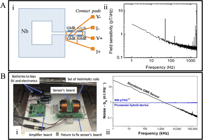
A (i) Schematic of the mixed GMR sensor structure. (ii) Noise spectra of the GMR sensor at 4 K. B (i) Experiment set up measuring the noise level. (ii) Noise spectrum of the hybrid sensor and the standalone GMR sensor. A Reprinted with permission from ref. 97, copyright 2011 AIP Publishing. B Reprinted from ref. 99, licensed under the terms of the Creative Commons Attribution License CC BY 4.0.
In addition to optimizing the structure of the GMR sensor, the reduction of 1/f noise can also be achieved by incorporating a microelectromechanical system (MEMS) flux concentrator98. Embracing this concept, Guedes et al. developed a hybrid GMR-MEMS device comprising magnetic flux concentrators (MFC) and MEMS cantilevers, achieving a device sensitivity of ~950 pT/Hz1/2 at 1 Hz99. The noise spectra of the hybrid sensor and the standalone GMR sensor were obtained using a testing setup illustrated in Figure 7B: i. A comparison of the noise spectra of these two sensor types in Figure 7B: ii indicates that the hybrid sensor has more than 10 times higher sensitivity compared to the standalone sensor at 1 Hz. The hybrid sensor was then tested in an unshielded environment to measure heartbeats, and the results were compatible with standard heart-rate monitors, further validating the potential use of the hybrid sensor for MCG.
GMR for neural signal recording
Similar to the way the electric activities of the heart muscle generate a bio-magnetic field, the electrical activities of neural cells also produce a bio-magnetic field as well. The signals generated by neurons are generally expected to have an amplitude in the range of 10–100 pT at a frequency of around 1 kHz100, which falls within the detectable range of GMR biosensors. Therefore, GMR-based biosensors also have the potential to serve as neural signal-recording devices101.
Amaral et al. demonstrated the first use of a GMR sensor to measure neural activities102. The device they employed featured an array of 15 GMR spin valve sensors with a field sensitivity of 0.15%/Oe. As illustrated in Fig. 8A: i, the giant magnetoresistive chip was positioned under a hippocampus slice of mice to measure the magnetic field generated by synaptic/action potential currents. Figure 8A: ii displays the readout of one giant magnetoresistive spin valve sensor after the hippocampus excitation in the CA3 region. The readout curve consists of pulses with an amplitude of 20 μV and a pulse length of 20–30 ms. To confirm that the detected signal is a real biological signal, two blockers were applied to the brain slice: the glutamate postsynaptic receptor blocker cyanquixaline (6-cyano-7-nitroquinoxaline-2,3-dione, CNQX) and the sodium channel blocker tetrodotoxin (TTX). The reduction of signal pulses shown in Fig. 8A: iii upon adding these blockers validates that the recorded pulses indeed originate from a biological source.
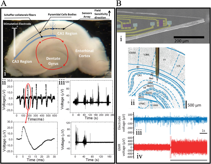
A (i) The structure of the hippocampus slice. (ii-iii) Recording of pulses without (ii) and with (iii) blockers. B (i) SEM image of the GMR probe. (ii) Schematic drawing of the position of the probe in the rat’s brain. (iii) Recording of electrode voltage. (iv) Recoding of the voltage of the GMR sensor near the tip. A Reprinted with permission from ref. 102, copyright 2011 AIP Publishing. B Reprinted with permission from ref. 104, copyright 2020 American Chemical Society.
In addition to the aforementioned in vitro tests, in vivo neuroactivity measurements have also been demonstrated using GMR sensors103,104. For in vivo testing, needle-type giant magnetoresistive devices are preferred as they can reduce damage to brain tissue during the insertion process and allow localized detection of specific areas of interest. For instance, Chopin et al. developed a 25-μm thick giant magnetoresistive needle device and achieved in vivo measurement of the brain activities of an anesthetized rat104. As depicted in Fig. 8B: i, the magnetic probe has two orthogonally placed GMR sensors on a silicon-on-insulator (SOI) wafer, with the tip at an angle of 18°. Phantom studies of this device yielded a sensitivity of 1.7%/mT along one axis and 0.9%/mT along the perpendicular axis in the sensor plane, with a detection limit at 1 kHz of 1.0 and 1.3 nT, respectively. During the real in vivo test process, the probe was inserted into the pyramidal cell layer of the dorsal hippocampus, as shown in Fig. 8B: ii. The large amplitude of extracellular spikes recorded in Fig. 8B: iii indicates successful probe placement at the right location. Magnetic spikes are not visible in the voltage trace of the GMR sensor, as shown in Fig. 8B: iv. This is an expected result, as the device’s limit of detection requires the signal to be averaged 42,500 times to achieve a reasonable signal-to-noise ratio.
Magnetic tunnel junction (MTJ)-based biomedical applications
Tunneling magnetoresistance (TMR) effect and MTJ devices
TMR effect
The tunneling magnetoresistance (TMR) effect was first observed in 1975 when M. Julliere established that the electrical resistance of the Fe-Ge-Co multilayer structure depended on the relative magnetizations of the Fe and Co ferromagnetic layers105. The key difference in the physical origin of GMR and TMR lies in the fact that GMR relies on conduction through a metallic conductive spacer layer, whereas TMR utilizes quantum tunneling through a very thin insulator layer, thus, resulting in significantly higher MR ratios.
The structure of magnetic tunnel junctions (MTJs) incorporates two ferromagnetic layers separated by a very thin insulator (I) layer, typically just a few nanometers thick (5–20 Å) to allow for the tunneling of electrons. However, this tunneling phenomenon is highly dependent on the alignment of electron spin with the spins of electrons in the respective ferromagnetic layers. That is, a high tunneling probability is achieved when most of the electron spin in both FM layers is aligned parallel and a low tunneling probability results from anti-parallel alignment of the majority electron spins in the FM layers. This process can be better understood with the DOS argument as schematically represented in Fig. 9.
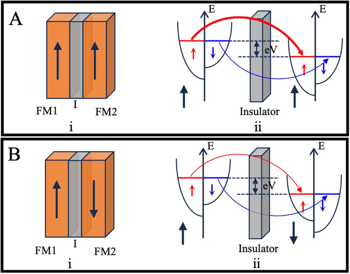
(A) parallel magnetization, and (B) antiparallel magnetization MTJ structures.
For a case where two FM layers have parallel magnetization, as shown in Fig. 9A: i, the spin alignment of the majority of spin electrons is also matched. Thus, electrons with the same spin as the majority spin in the first layer can easily tunnel to the majority spin band of the second layer as captured in Fig. 9A: ii. Whereas the minority spin electrons from FM1 can only tunnel to the minority spin band of FM2. This corresponds to a low resistance state (RP) and thus results in a high current flow through the MTJ. In a scenario where the magnetizations of two FM layers are aligned antiparallel as shown in Fig. 9B: i, majority spin electrons from the first FM layer can only enter the minority spin bands in the second FM layer. Similarly, the minority spin electrons that have a low DOS in the first FM layer can only tunnel to the majority DOS in the second FM layer as depicted in Fig. 9B: ii. This results in a high resistance state (RAP) and thus low current flow through the MTJ structure. The TMR ratio for MTJ devices is thus defined by the equation:
MTJ devices
MTJs find a variety of applications ranging from memory, computing, current, and position sensing to biomedical applications. However, in the context of this work, we will limit our discussion to the MTJ sensors targeting biomedical applications. In such cases, MTJs constitute a spin-valve structure where one of the ferromagnetic layers is fixed (pinned), i.e. its magnetization direction does not change, whilst the other layer is free (unpinned) and can change its magnetization depending on an external field. A typical spin-valve structure along with its R-H (resistance change with applied field) response curve is presented in Fig. 10A: i, ii respectively. Targeting the biomedical applications of MTJ-based devices, the key focus of the sensor development lies in achieving a wide dynamic range (i.e. linear range), high sensitivity, and improved noise performance. MTJ-based sensors exhibit non-linear R-H response curves when the free and pinned layers have parallel magnetization directions. This results in a large amount of magnetic field being needed to change the sensor’s state (coercivity). To achieve a linear R-H response, MTJ-based sensors having crossed (relatively perpendicular) anisotropies of the free and pinned layer are designed. This can be achieved by different linearization strategies106 such as (i) utilization of shape anisotropy of MTJ-based device structure, (ii) weakly pinned sensing layer, (iii) external biasing of the free layer, and (iv) designing superparamagnetic sensing layer. External biasing of the free layer requires adaptation of magnetic structures into design thus increasing the area cost. Whereas superparamagnetic sensing layer structures are better suited for current and position sensing industrial applications where a large linear range (sub-mT) is required. Thus, shape anisotropy107,108,109,110,111,112,113 and weakly pinned sensing layer114,115,116,117,118 linearization strategies are the most commonly used for biosensing applications due to higher sensitivity and simpler stack implementations.
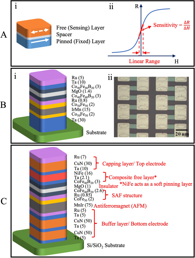
A (i) Spin valve structure depiction. (ii) A representative R-H curve of a TMR sensor. B (i) Stack design for an MTJ device with linearity due to shape anisotropy. (ii) A close-up optical image of MTJ sensor elements showing the elliptical geometry used for achieving the shape anisotropy. C MTJ stack design with weakly pinned sensing layer for achieving hysteresis-free and linear R-H response curve. B (i) is originally plotted by the authors based on the MTJ stack design described in ref. 109. B (ii) Reprinted with permission from ref. 109, copyright 2008 AIP Publishing. C is originally plotted by the authors based on the MTJ stack design described in ref. 118.
The pinned layer implementation in MTJ stack design is achieved using antiferromagnet (AFM) and synthetic antiferromagnetic structures (SAF). A reference design for an MTJ-based linear device with shape anisotropy as developed by Shen et al. for DNA detection application109 is presented in Fig. 10B: i. The thickness of different thin films deposited for the stack design is mentioned in brackets with measurement units in nanometer (nm) scale. The magnetization direction in the reference layer (Co40Fe40B20) is fixed by way of RKKY (Ruderman–Kittel–Kasuya–Yosida) coupling with the Co50Fe50 thin film. The use of a thin Ru layer facilitates this RKKY coupling between the Co40Fe40B20 and Co50Fe50 by forming a synthetic antiferromagnet (SAF) structure. IrMn layer is used to fix the magnetization direction of the Co50Fe50 thin film through anti-ferromagnetic interactions. The MTJ nanopillars were patterned in an elliptical geometry of lateral dimensions 6 × 18 µm each as shown in Fig. 10B: ii. The geometry thus results in a shape anisotropy needed for crossed anisotropies of the free and reference layers and thus the linearized device output behavior.
In a soft-pinning linearization structure, the free layer magnetization is stabilized with a weak pinning force perpendicular to the reference layer magnetization. This soft pinning is achieved by the use of a composite-free layer. A reference design based on the MTJ stack developed by Amaral et al. for magnetic measurements of neuron signals118 has been presented in Fig. 10C. Like the previously described structure, the AFM layer and SAF interactions were utilized for fixing the magnetization alignment of the pinned layer. A composite-free layer constituting NiFe(16) / Ta(2.1) / CoFe40B20(3) is utilized to ensure a linearized R-H response. Here NiFe layer provides the soft pinning needed to maintain relative crossed anisotropies of free and the sensing layer at zero applied fields and the Ta spacer is used to ferro-couple the NiFe and CoFe40B20 layers.
To achieve high device sensitivities and improved sensor resilience, the MTJ-based sensors are often configured in a Wheatstone bridge implementation with one variable arm115,116. The inclusion of magnetic flux concentrators (MFCs) in MTJ-based devices improves their sensitivity significantly by amplifying the magnetic field experienced by individual sensing elements116,117. They act as funnels, channeling and concentrating the external magnetic field onto the MTJs. Some of the other notable trends to improve the MTJ-based device sensitivities include engineering composite sensing layer and spacer structures such as CoFeSiB sensing layer119,120 and TaFeB spacer designs121. The noise performance of MTJ-based sensors is also inversely coupled with the device sensitivity. An increase in the device sensitivity results in poorer noise performance, thus a trade-off must be established according to the application of interest. The key components influencing the noise performance include (i) 1/f noise – arising from inherent device imperfections and charge trapping, (ii) shot noise – due to random fluctuations in the current flow, and (iii) thermal noise – pertaining to thermal vibrations of atoms resulting in resistance fluctuations. Due to the limited scope of this work, a better discussion can be found in prior published art122,123.
MTJ-based bioassays
Over the last 20 years, there has been a notable increase in the number of applications for magnetic field biosensors28. Among the other magnetic sensors, the MTJ-based room temperature sensor with a barrier layer is the most extensive discovery that can achieve a detection limit near the sub-pT range122,124,125,126,127. For instance, Li et al.107 present the HIV-1 (p24) antigen detection with sandwich bioassays using the MTJ-based biosensor with thin film stack designs shown below: substrate/Ta(5)/Ru(30)/Ta(5)/CoFe(2)/IrMn(15)/CoFe(2)/Ru(0.8)/CoFeB (3)/MgO(1.9)/CoFeB (3)/Ta (5)/Ru (10), numbers in brackets are in nm. The identification of target p24 biomolecules was achieved using a two-point probe measuring setup with an MTJ-based array sensor and biofunctionalized iron oxide MNPs. Differentially comparing the tunnel magnetoresistance sensor’s signal to its reference, the signal from the designated MNPs was ascertained. For the p24 antigen with the concentration change of 1 μg/ml, there is a resistance variation ΔR = 74 ± 6 Ω in the sensor easy axis, which was reported to determine the biomolecule.
Sharma et al. have shown how to use the MTJ structure to extract natural DNA from pathogenic bacteria such as Salmonella, Listeria, and Hepatitis E. virus (HEV), and to detect these bacteria at concentrations lower than 1 nM using an MTJ thin film stack of Ta(5)/Ru(18)/Ta(3)/Ir20Mn80(20)/Co60Fe40 (1.8)/ u(0.9)/Co40Fe40B2(2.7)/MgO(2.5)/Co40Fe40B20 (1.3)/Ru(5)/Ta(20), numbers in brackets are in nm128. The fabricated MTJ sensors are shown in Fig. 11A. They presented a compact portable device containing 12 MTJs. Half of the MTJs were immobilized with the complementary probe and the other half (control sensors) with noncomplementary probes. The control sensor is used to monitor the washing step (removing the non-bound beads) to observe when the signal returns to baseline. In their device, the orthogonality of DNA probes enables the possibility of multiplexed assays, where the simultaneous assessment of multiple pathogens in a single assay is feasible due to the probes’ ability to bind without cross-reactivity selectively. Finally, for experimentally demonstrating the detection of natural DNA hybridization of Listeria, the sensor is hybridized with 1 μM and 1 nM concentrations of Listeria target DNA.
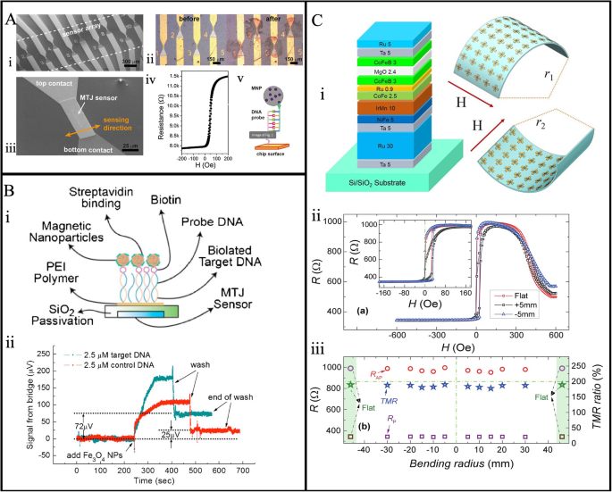
A MTJ sensor arrays of 12. (i) SEM images with common ground contact. (ii) Before and after optical images of the Listeria DNA (100 nM target) detection. (iii) Zoom-in view of one MTJ covering a 40 × 3 μm2 area. (iv) MR response of the MTJ sensor. (v) The streptavidin bound with biotinylated target DNA detection scheme of MNP. B (i) MTJ bioassay arrays surface immobilization schematic. (ii) The real-time detection of 2.5 μM target DNA (cyan) and the 2.5 μM control DNA (red) using the sensor. C (i) Schematics of MTJ blocks and flexible wearable configuration with bending structure and the effect of bending (ii) for positive and negative bending radius of 5 mm. (iii) Effect of the bending on the parallel and antiparallel resistance. A Reprinted with permission from ref. 128, copyright 2016 Elsevier B.V. B Reprinted with permission from ref. 109, copyright 2008 AIP Publishing. C Reprinted from ref. 129. licensed under the terms of the Creative Commons Attribution License CC BY 4.0.
Similarly, Shen et al.109 demonstrated the detection of 2.5 μM target DNA using the 16 nm MNPs with the tunnel magnetoresistive biosensors, depicted in Fig. 11B. They have demonstrated the real-time detection of the complementary target DNA and the noncomplementary control DNA in Fig. 11B: ii. Phosphate-buffered saline (PBS) is initially flushed through the fluid channel to stabilize the system before the MNPs are added. The graph in Fig. 11B: ii illustrates how binding occurs for target DNA, reaching saturation points at around 180 μVrms. Subsequently, PBS is flown again to eliminate unbound MNPs from the MTJ array surface, presenting a residual signal of 72 μVrms. However, because of the nonspecific interaction between the MNPs and the polymers, there is some residue signal for the 2.5 μM MNPs containing control DNA, even though in an ideal situation, there should not be any residue signal left over after hybridization processes. Thus, they have demonstrated how to determine the target DNA concentration by analyzing the output signal.
Furthermore, Mu et al.114 presented the rapid detection of ricin in water, soil, food, blood, and so on using the MTJ-based sensor having a core structure of Si/SiO2 substrate/Buffer layer/PtMn/CoFe/CoFeB (3)/MgO (2)/CoFeB(3)/NiFe/IrMn/Capping layer, numbers in brackets are in nm. In their study, they combined the MTJ-based sensor with a test stripe of the magnetic immune chromatographic to detect the presence of ricin. The immune chromatographic magnetic test trip was prepared with the carboxyl-modified superparamagnetic Fe3O4 nanoparticles (250 μL, 4 mg/mL) with the anti-ricin monoclonal antibody by EDC-NHS from an NHS-active ester group. The detection process was placing the solutions with various concentrations of 1 ng/mL to 20 μg/mL in the sample hole of the test stripe. Then, the membranes were observed to determine the stripes appearing on the test line and control line. After that, the test line and control line output voltage were measured, and later, the ricin samples were replaced by a PBS buffer to remove the unbound MNPs to obtain the background voltage. Thus, the concentration of ricin was ascertained quantitatively by monitoring the voltage change.
Chen et al. reported the flexible and wearable MTJ on ultrathin (14 μm) silicon substrates illustrated in Fig. 11C129. In this flexible sensor, the MTJ’s performance does not degrade while cyclically bent about 500 times the radius of 15 mm in both positive and negative directions. Figure 11C: ii shows that the tunnel magnetoresistive loops were slightly varied due to bending, which is due to the residual stress. However, the TMR ratio did not degrade under 1000 bending cycles, remaining at 189 ± 4% as shown in Fig. 11C: iii. This flexible electronics biosensing will surely open doors for new wearable biosensing. Nevertheless, the top electrodes of MTJ-based sensors are frequently thicker compared to GMR sensors. This results in a smaller sensing field for the free layer, consequently restricting its potential applications. Additionally, the inherent high noise level in MTJ-based sensors poses a challenge in achieving ultra-high sensitivities that must be overcome.
MTJs for magnetocardiography (MCG)
MTJ-based sensors typically exhibit an MR ratio one order of magnitude higher than giant magnetoresistive sensors, resulting in greater sensitivity. This characteristic makes MTJ sensors well-suited for magnetocardiography applications130,131. However, similar to GMR-based sensors, MTJ-based sensors face challenges associated with high 1/f noise. The issue is exacerbated in tunnel magnetoresistive sensors due to charge trapping in the insulation layer and at the interfaces, posing a more severe obstacle to their optimal performance132,133.
As discussed in Section “GMR for Magnetocardiography (MCG)”, MEMS have been integrated into giant magnetoresistive sensors to mitigate 1/f noise. This same approach has been extended to MTJ-based sensors for MCG applications. For instance, Oogane et al. developed an MTJ-based device for detecting sub-pT magnetic fields, showcasing its real-time MCG measurement capabilities117. As illustrated in Fig. 12A: i, the device comprises 74 MTJ sensors connected in series. T-shaped MFCs were affixed to both sides of the MTJ array, effectively enhancing the flux density of the external magnetic field. The detectivity spectrum, depicted in Fig. 12A: ii, reveals that the incorporation of MFCs led to a reduction in noise level, achieving detectivities of 0.94 pT/Hz1/2 at 1 Hz and 50 fT/Hz1/2 at 1 kHz. MCG measurements were carried out by placing the MTJ device on the chest, as illustrated in Fig. 12A: iii. The real-time measurement results are presented in Fig. 12A: iv, where the extended period is attributed to body movements induced by respiration. To mitigate this effect on the signal, a digital filter was applied from 10 to 30 Hz. The filtered signal, shown in Fig. 12A: v, exhibits clear QRS components.
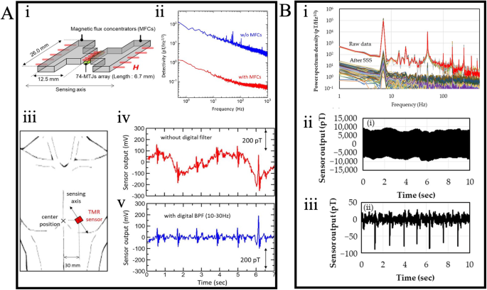
A (i) Schematic figure of the MTJ sensor array and MFCs. (ii) Detectivity spectrum of the MTJ device with and without MFCs. (iii) Schematic illustration of the device position for MCG measurements. MCG spectrum without (iv) and with (v) a digital bandpass filter (DBF). B (i) Power spectrum density of the device before and after SSS processing. MCG measurement results before (ii) and after (iii) applying SSS and digital filter. A Reprinted from ref. 117, licensed under the terms of the Creative Commons Attribution License CC BY 4.0. B Reprinted from ref. 116, licensed under the terms of the Creative Commons Attribution License CC BY 4.0.
In addition to directly suppressing the 1/f noise generated, an alternative approach to effectively reduce the noise level and enhance the signal-to-noise ratio of the MTJ-based MCG sensor involves employing advanced data and signal processing techniques during a post-signal collection stage134,135,136. One such method, proposed by Sakib et al., utilizes an artificial intelligence model known as reservoir computing (RC) to effectively eliminate 1/f noise from the MCG signal136. Their simulation results demonstrate that the RC model can significantly reduce 1/f noise with minimal error, requiring lower training time and memory.
The application of sophisticated mathematical models to mitigate environmental noise has also seen significant advancements. Kurashima et al.116 implemented a signal space separation (SSS) technique in their MTJ-based sensors, resulting in the successful reduction of environmental magnetic noise. To assess the performance of SSS, a Helmholtz coil generating a magnetic field of 100 nTp-p at 7 Hz was placed near the MTJ-based sensors. Figure 12B: i illustrates the power spectrum density, indicating a notable noise reduction of approximately −73 dB at 7 Hz post-SSS processing. Moreover, a comparison of MCG measurement results before and after applying SSS and a digital filter is presented in Fig. 12B: ii, iii. The results demonstrate that digital processing significantly diminishes environmental noise, reinforcing the potential to forego the use of physical magnetically shielded rooms through the application of advanced signal processing methods.
MTJs for neural signal recording
It is difficult to properly comprehend how the brain functions because it is a complicated neuronal network connected by synapses. The primary units that link and interact with each other among the neurons are the action potentials (illustrated in Fig. 13A). As of right now, brain electric fields and information exchange are well understood137,138, but the magnetic activity of neurons is still mostly unknown. This is because of technical challenges that arise while recording extremely weak signals from the neurons. Thus, wirelessly detecting this action potential with high temporal and spatial resolution would be excellent for processing information and curing neurological diseases139. Research has been carried out on applying MTJ-based sensors to record neural signals.
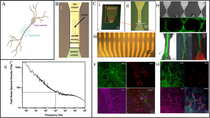
A Pyramidal neuron and the electric currents (purple) and magnetic fluxes (turquoise) illustration. B (i) MTJs sensor arrays (12) with separate top and bottom contact optical images and (ii) field noise spectral density measurement. C 12-MTJ sensor array optical image (i), the single sensor (ii), zoomed image in area 4 × 30 μm2 (iii), rat hippocampal neurons images obtained with fluorescence microscope where the neurons are growth with controlled engineered tropology for best system sensitivity (iv), and primary rat hippocampal neurons grown with random topology (v) on the top of MTJ sensor; (vi) neurons grown outside the sensor surface of active region. A Reprinted from ref. 177, licensed under the terms of the Creative Commons Attribution License CC BY 4.0. B Reprinted from ref. 112, licensed under the terms of the Creative Commons Attribution License CC BY 4.0. C Reprinted from ref. 113, licensed under the terms of the Creative Commons Attribution License CC BY 4.0.
For instance, Amaral et al. created a microneedle that measures the neural activity in a mouse hippocampal brain slice by integrating the MTJ-based sensor with Si118. Because these Si microneedles are made with precise geometric measurements and have an MR sensor attached to the tip of each needle, they may be implanted into a brain slice without inflicting any major damage. The MR sensor-mounted needles are placed on a micro-positioner and moved to the mouse brain slice’s region of interest. The pulse is measured from the pyramidal cell bodies region with the MTJ-based sensors array after the hippocampus excitations in the CA1 region. Likewise, Sharma et al. presented tunnel magnetoresistive sensor arrays for detecting the hippocampal brain slice neural culture on the sensor surface (sensor shown in Fig. 13B: i)112. Since the brain action potential lasts one millisecond, the correlation spectrum analyzer was utilized to compute the spectrum in the 1 kHz range presented in Fig. 13B: ii. The noise spectrum density of their system was found to be approximately 5 nT/Hz1/2. Moretti et al. cultivated the neurons on the MTJ-based sensor surface to illustrate the MTJ sensor for in vitro applications113, as depicted in Fig. 13C. By allowing the neurons to grow on top of the MTJ-based sensor surface for 20 days, they were able to demonstrate the magnetic properties of the neurons and showcase that there are no constraints. They were also able to successfully grow neural networks with controlled topology, proving the biocompatibility of the MTJ-based sensor chip for neural activities. Moreover, comparable outcomes are shown when neurons grown onto MTJs with controlled and uncontrolled tropology are evaluated. Recently, Algarin et al. showcased that action potentials from crayfish-isolated nerve cords could produce microwave signals in nanopillar MTJs (NMTJs), and their NMTJ-based device has both the sensitivity and temporal resolution to respond to action potentials from a single neuron111. Moreover, their developed NMTJ can be used in minimal surface areas (nanoscale), and operating at a shallow input current would surely be impactful for low-power wireless sensor arrays.
Anisotropic magnetoresistance (AMR)-based biomedical Applications
AMR effect and devices
The anisotropic magnetoresistance (AMR) sensor was first demonstrated by William Thomson, dating back to 1857, before GMR and MTJ-based sensors were reported140. In comparison to giant magnetoresistive and MTJ structures, the fabrication of anisotropic magnetoresistive devices is relatively straightforward, presenting significant potential in data storage141, navigation142, medical diagnostics143,144,145, and many more applications146,147,148,149,150. The AMR effect occurs due to the variation of the in-between angle of the external magnetic field and the conduction current direction. This deflection in the conduction current direction originates from the asymmetry of the electron orbits and the anisotropic scattering of the conduction electron due to spin-orbital interaction (SOI)151 in the ferromagnetic material as this induces the asymmetry of the electron orbits. The ferromagnetic material’s atomic configuration exhibits that the 3d band is not filled. Consequently, in the presence of an applied magnetic field, the 4s electrons tend to get scattered into the sub-bands of 3d orbits152. This electron orbit asymmetry affects the conductivity of electrons traveling either perpendicular or parallel to the applied magnetic field, giving rise to magnetoresistance. Hence, the maximum resistivity (({rho }_{parallel })) is observed when the current and the magnetization are parallel to each other, i.e., θ = 0o. and contrastingly, when the current and the magnetization are perpendicular, θ = 90o, the minimum resistivity is obtained (({rho }_{perp })), as illustrated in Fig. 14B. The resistance dependence with the relative angle can be defined as follows:
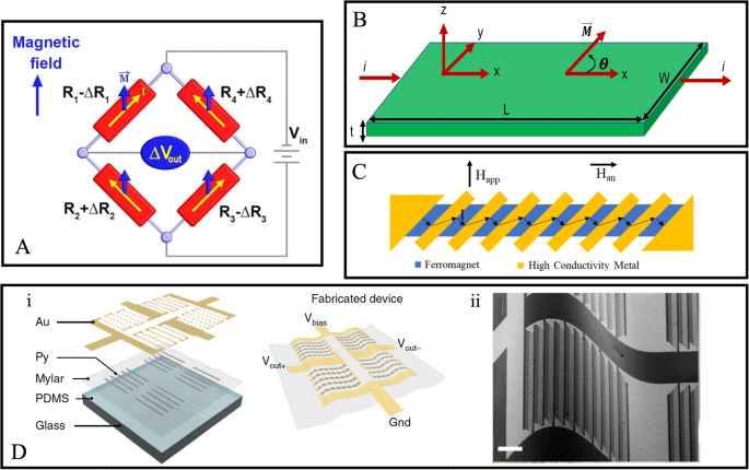
A AMR Whiston bridge diagram. B AMR thin film schematics. C The barber-pole structure twisted the current direction at an angle to the anisotropy field to achieve linear magnetoresistance. D (i) The fabrication schematics of the AMR-based e-skin compass, (ii) The SEM image of the device under 200 μm of bending radius. A Reprinted with permission from ref. 155. copyright 2018 The Minerals, Metals & Materials Society. B is originally plotted by the authors. C Reprinted from ref. 153, licensed under the terms of the Creative Commons Attribution License CC BY 4.0. D Reprinted with permission from ref. 158, copyright 2018 The Author(s), under exclusive licence to Springer Nature Limited.
The ferromagnetic material resistance changes nonlinearly with the external field153. So, to make this effect linearize the barbel pole structure shown in Fig. 14C where the conducting current direction bends at a 45o angle concerning the easy axis of the ferromagnetic material. It is realized by placing a conductor of gold or aluminum material at a 45o angle to the FM layer, which forbids the current from flowing directly to the easy axis of the ferromagnetic layer, resulting in more linear resistance for the applied field154.
Quynh et al. reported the Wheatstone bridge sensor based on the AMR effect using the NiFe (permalloy) arms (R1, R2, R3, and R4) shown in Fig. 14A155. They show that high sensitivity is improved using the Wheatstone bridge connection, and the thermal noise is reduced. Furthermore, Guo et al. used the Wheatstone bridge configuration and highlighted that the narrower barber pole bar size means reduced unchanged resistance component with applied field results in an improvement in the MR curve156. In addition, Ritzinger et al. discussed the presence of negative AMR in transition metal alloys with aluminum157. Recently, Bermúdez et al. presented the flexible AMR-based electronic skin (E-skin) compass fabricated on 6-μm thick polymeric foils, which is capable of detecting earth magnetic field up to 40–60 μT and immune to bending even below 200 μm of bending radius158. They fabricated the e-skin AMR sensor onto a rigid PDMS-coated glass slide, which is laminated using the Mylar foils, and the sensing layer having 50 nm thickness is based on ferromagnetic stripes of Permalloy (Py, Fe81Ni19 alloy) and the gold with 100 nm thickness is used to cap the contact and conditioning layer. Notably, this high mechanical bending immunity is achieved with ultrathin thick Mylar foils and reported to have 25 times higher bendability than other reported flexible AMR sensors showcased in Fig. 14D. Although the recent AMR with NiCo and NiFe materials improved the AMR values to 7% compared with the conventional Fe, Ni, and Co (their AMR was only 2%) at room temperature, its sensitivity is not nearly comparable with GMR and MTJ devices. However, it served as an indispensable role in the early development of magnetoresistive sensors159.
AMR-based bioassays
Miller et al. first introduced a ring AMR-based biosensor design with Ni80Fe20 material utilizing modulation of AMR using radial fringing field shown in Fig. 15A160. In the absence of a magnetic bead, the current flows parallel and antiparallel to the magnetization. Therefore, the highest anisotropic magnetoresistance is observed. When a magnetic bead is present, the parallel and antiparallel magnetic fields rotate to the radial direction which is perpendicular to the current, resulting in reduced resistance. Additionally, the AMR response is contingent on the magnetic bead’s position, as the peaked AMR response occurred when the bead was precisely above the ring, and as it moved outside, the signal reduced to zero. This discovery made it a potential magnetic sensor for a broad spectrum of biological applications related to magnetic disposable cards161 and genotyping162.
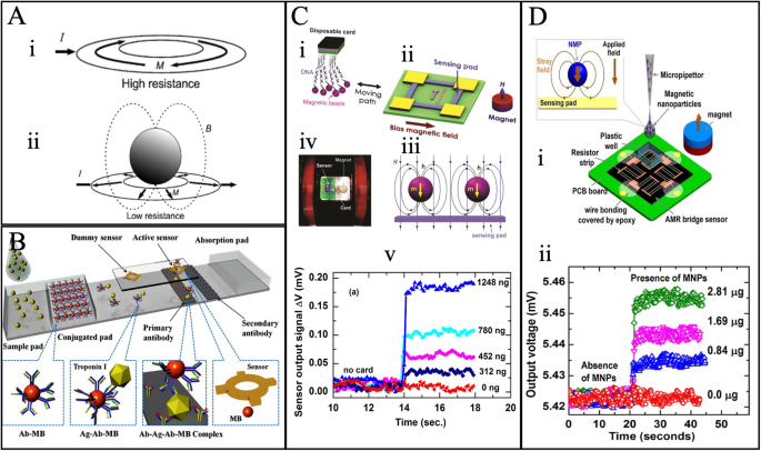
A AMR ring resonator diagram having maximum resistance (i). Due to the presence of MNPs, the resistance is reduced to minimum resistance (ii). B Numerical modeling of nitrocellulose (NC) membrane detection using AMR/PHR hybrid sensor. C The disposable card detection experimental setup (i-iv) and the sensor recorded magnetic particle signals (v). D (i) MNP detection using a combination of six series and parallel resistors sensor and (ii) Voltage signal regarding the presence and absence of MNP of Fe3O4-chitosan. A Reprinted with permission from ref. 178, copyright 2008 Elsevier B.V. B Reprinted with permission from ref. 161, copyright 2011 Elsevier B.V. C Reprinted from ref. 163, licensed under the terms of the Creative Commons Attribution License CC BY 3.0. D Reprinted with permission from ref. 155, copyright 2018 The Minerals, Metals & Materials Society.
Oh et al. demonstrated the Cardiac Troponin I (cTnI) immunomagnetic beads (e.g., it contains antigen, antibody, and magnetic beads complex (Ag-Ab-MB)) and their binding kinetics detection by the flowing membrane in an AMR and planar hall resistance (PHR) based hybrid ring sensors (e.g., shown in Fig. 15B)161.Hien et al. developed an AMR-based disposable card for detecting specific magnetically labeled DNA163. It focused on particular DNA probes for targeting the 16S rRNA gene of Streptococcus suis, shown in Fig. 15C. The DNA probe was synthesized using genetic information obtained from the Gene Bank at the National Center for Biotechnology Information (NCBI) and a DNA sequence alignment program. The DNA was magnetically labeled using superparamagnetic, and the number of magnetic beads was measured using a vibration sample magnetometer (VSM). Ultimately, these magnetic DNA were detected with a permanent magnet magnetic field and the AMR sensor with the Whitestone bridge configuration. Figure 15C: iii shows the DNA magnetic stray field and permanent magnet field. Furthermore, Fig. 15C: v shows the real-time detection of output voltage with different amounts of MNPs, whereas its detection limit is 3.8 μemu. The disposable card seems to give higher efficiency and performance with the immobilization of bioassays and is cost-effective for biomedical applications. Most recently, Quynh et al. in 2019 proposed a new design (e.g., Fig. 15D) containing series and parallel resistance connection using Ta (10)/Ni80Fe20 (5)/Ta (10) films that show significant improvement in the detection limit up to 0.56 μemu155. Fig. 15D: ii illustrates the output voltage signal regarding the MNP of Fe3O4-chitosan. Additionally, the flexible AMR device on a polyethylene terephthalate (PET) substrate was fabricated by Wang et al., demonstrating negligible output voltage degradation up to 5 mm bending radii164. Even though enough research has been made to improve AMR sensitivity for MNP detection compared to performance of GMR-based and MTJ-based devices, it remains limited to a few lateral flow immunoassays (LFIA) sample detection.
Challenges and opportunities
The development of MR (e.g., GMR, MTJ, AMR) biosensors for biomedical applications faces several complex challenges and is shaped by emerging trends in sensor technology. One significant hurdle is achieving a low detection limit while simultaneously maintaining cost-effectiveness. Researchers have explored various strategies to enhance sensitivity, including the integration of MR biosensors with MEMS and MFCs. However, this integration introduces additional complexities in sensor design, leading to challenges in fabrication and increasing the overall cost per chip. Balancing the need for high sensitivity with cost considerations remains a critical focus in the field.
Another key trend in MR biosensor development is the transition towards on-field applications outside traditional laboratory and clinical settings. While GMR-based biosensors have shown promising results in point-of-care (POC) devices, achieving widespread commercialization has proven challenging. The move towards on-field applications demands biosensors that are not only highly sensitive and accurate but also user-friendly and fully automatic. This necessitates the development of intuitive interfaces and automated processes, reducing the need for extensive training and expertise among users. Moreover, ensuring the reliability and stability of biosensor performance in real-world, dynamic environments poses additional challenges that must be addressed to enable successful deployment in on-field settings. For example, deployment of MR sensors in on-field settings can introduce frequency-independent noise such as thermal or Johnson-Nyquist noise, 1/f noise, connection noise between device and electrodes, random telegraph noise (RTN), as well as non-magnetic noise caused by the external environment165. Moreover, the thermodynamic fluctuation causes electrical noise, which is also known as junction noise, which is expressed as (leftlangle {V}_{J}rightrangle =sqrt{({kT}varDelta {fR})}) where the k is Boltzmann constant, T is temperature, and (varDelta f) is the frequency, and R is the resistance166. So, from the expression, it is obtained that the Johnson noise drastically limited the detection at high frequencies.
All these noises, combined with the intrinsic MR device noise, led to the noise floor frequently reported by researchers. For instance, Silva et al. reported that connecting giant magnetoresistive SVs in parallel and series, a general noise reduction strategy, can improve the field detectivity in the thermal noise limit from 39 pT/(surd)Hz to 12 pT/(surd)Hz. With the variations of measurement environment, external circuitry, etc., the detectivity of GMR sensors spans a wide range from 0.1 to 10 nT/(surd)Hz @ 1 kHz38,99. Similarly, MTJs are reported to show field detectivities from 576 pT/(surd)Hz @ 100 Hz in ref. 45,126. pT/ (surd)Hz @ 10 Hz in ref. 124. Also, for AMR sensors, low noise detectivities are reported, such as in the white noise region, Enger et al. showcased as low as 1.4 nT/ (surd)Hz @ 1 Hz and 240 pT/(surd)Hz operating at 310 K167. They also reported that the performance beyond 1 kHz is comparable with that of giant and tunnel MR multilayer devices employing metallic ferromagnetic materials. Similarly, Nhalil et al. reported the elliptic planer hall effect (PHE) based sensor showcasing equivalent noise ratio of ~5 pT/(surd)Hz at 10 Hz, 7.4 pT/(surd)Hz at 1 Hz, and below 100 pT/(surd)Hz at 10 mHz in the room temperature and would be useful for detecting as low as sub pT range168. The primary parameters of operating the magnetic sensors are the signal drift due to the thermal fluctuations, sensitivities, and operating field range169. For instance, if the temperature change causes the resistance to be changed to much higher than the MR percentage, then the temperature drift of the sensor will get higher than the sensor’s signal amplitude. To solve this problem, the MR percentage must be increased, or the drift must be decreased. Thus, sensors need to operate with thermal stability. Finally, Table 1 illustrates a comparative study of the GMR, AMR, and TMR sensors operating at different temperatures as well as the low-frequency 1/f noise dominance.
Furthermore, cost per chip remains a significant barrier to the widespread adoption of MR biosensors, particularly in resource-limited areas where affordability is paramount. The fabrication processes involved in producing nano/micro-sized sensor device arrays contribute significantly to the overall cost per chip. As such, efforts to optimize fabrication techniques and reduce manufacturing costs are crucial for improving accessibility to MR biosensor technology, particularly in regions with limited financial resources. Additionally, ensuring consistent sensor-to-sensor, chip-to-chip, and batch-to-batch repeatability is essential for achieving reliable and reproducible results in biomedical applications. Addressing these challenges and trends will be instrumental in advancing MR biosensors, paving the way for their broader utilization in diverse biomedical applications and facilitating improved healthcare outcomes.
Conclusive remarks
In this work, we provided an up-to-date technology review on some popular spintronic devices, specifically focusing on GMR, TMR, and AMR effects, with an emphasis on their applications within the burgeoning field of biomedical technologies. Table 2 summarizes the bioassays based on these MR biosensors. We first reviewed three types of giant magnetoresistive structures such as multilayer GMR-based devices, GMR-based spin valves, and granular GMR effects. With the emerging designs of flexible GMR sensors, we have also covered printable designs, highlighting their inherent versatility and potential for seamless integration into diverse biomedical applications. With over 30 years of study on GMR, stack design optimization170, and integration with multiple technologies171, GMR-based technology exhibits a higher level of detectivity compared to AMR yet falls short of the superior detectivity offered by MTJs, and the fact that GMR-based devices are less susceptible to interfacial roughness and crystalline defects over MTJs172,173,174. GMR stands out as the preferred choice among all MR sensors for bioassays, we have showcased some representative GMR-based bioassay works drawn from existing literature. In the domain of MCG, a non-invasive diagnostic tool crucial for measuring the bio-magnetic field generated by the heart’s electrical activities, we have highlighted the limitations of conventional methods relying on SQUIDs. In this context, both GMR and MTJ-based sensors emerge as promising alternatives, with innovative structural configurations like Wheatstone bridges and MFCs enhancing their on-chip detection capabilities for ultra-low magnetic fields. We have also covered the applications of GMR and TMR sensors in neural signal recording, addressing the intricate challenge of capturing neurological activities, especially at the single neuron level. Several groups around the globe have successfully recorded neuron activities using specially designed GMR and TMR sensors, emphasizing their heightened sensitivity and relevance in this complex domain.
Despite knowledge of AMR predating the advent of GMR and TMR, its constrained MR ratio has delimited its application as magnetometers, particularly in biomedical settings characterized by low bio-magnetic fields and magnetic stray fields from magnetic labels. Notwithstanding recent strides in improving AMR values through the incorporation of NiCo and NiFe materials, its sensitivity remains markedly inferior to that exhibited by GMR-based and MTJ-based devices. However, it is imperative to acknowledge the historical significance of AMR in the nascent stages of MR sensor development.
The increasing demand for highly sensitive magnetic field sensors catering to quantitative bioassays, MCG, and neural signal recording fuels the ongoing evolution of magnetic biosensors. Consequently, as these devices continue to advance, the prospect of attaining unprecedented precision in the acquisition and interpretation of biomedical signals portends the opening of novel frontiers for diagnosis, monitoring, and comprehension of intricate physiological processes.

Responses