Strain-dependent charge trapping and its impact on the operational stability of polymer field-effect transistors

Introduction
With the increasing importance of stretchable and flexible electronic devices as human-machine interfaces, the utilization of semiconducting polymers in field-effect transistors (FETs) has attracted considerable interest because of their mechanical stretchability and solution processability. As a result of extensive research, a high degree of mechanical stability has recently been achieved for some organic field-effect transistors (OFETs) with superior charge carrier mobility; the field-effect charge carrier mobility of stretchable OFETs has exceeded 1 cm2 V−1 s−1, which surpasses that of inorganic FETs based on amorphous Si or metal oxides while maintaining the OFETs’ stretchability1,2,3,4,5,6. However, in contrast to the recent progress in achieving high mechanical stability of stretchable OFETs, their bias-stress stability problems have not received much attention and remain a bottleneck for the commercialization of stretchable OFETs7,8,9,10,11,12.
In OFETs, bias-stress stability is observed as a shift in the threshold voltage (Vth) and a decrease in the drain current (ID) under continuous electrical biases applied to the devices over a prolonged period13,14,15. Numerous studies have been conducted to elucidate the origin of the bias-stress instability of OFETs7,15. In general, bias-stress instability is attributed to charge trapping within OFETs; the trapped electrons/holes distort the current flow and electric potential distribution within the devices, resulting in a shift of the Vth and a decrease of the ID. There are different sites for charge trapping, including sites at the gate dielectric–organic semiconductor interface and within the organic semiconductor layer. There are also different sources of charge trapping, depending on the trapping mechanisms. For example, charge trapping in the organic semiconductor layer can arise from its intrinsic structural disorder16,17,18 or from its chemical interactions with external sources such as molecular oxygen or water19,20,21,22,23,24. Charge trapping at the gate dielectric–organic semiconductor interface can arise from electrochemical reactions at the interface (e.g., the formation of Si–O− groups via electron trapping at the SiO2–organic interface)25.
Although the contributions of numerous studies have led to a deep understanding of the mechanisms of charge trapping and their effects on the bias-stress stability of OFETs, these studies have primarily focused on unstretched devices. Research into the bias-stress stability of OFETs under nonzero strain has been rare. Stretching an OFET device is expected to cause substantial structural changes in the layers comprising the device, leading to considerable changes in the charge trapping behavior and bias-stress stability of the device. Therefore, to achieve stretchable OFETs with high bias-stress stability, understanding the correlation among changes in the microstructures of the constituent films, charge trapping, and the bias-stress stability of OFETs under mechanical strain is important.
In the present work, we investigated the effect of mechanical strain-induced microstructural changes of semiconducting polymer thin films on the charge trapping behavior and bias-stress stability of the corresponding polymer FETs. The donor–acceptor–type copolymer indacenodithiophene-co-benzothiadiazole (IDTBT), a representative low-crystalline polymer with high charge carrier mobility, is used as a model semiconducting polymer. We found that the bias-stress stability of IDTBT-based FETs strongly depends on the strain applied to the IDTBT film, showing poorer bias-stress stability when the polymer film was subjected to greater strain. Photo-excited charge collection spectroscopy (PECCS) was performed to quantify the trapped charge density within the devices under different strains and to investigate the charge-trapping mechanism. As a result, we showed that the bias-stress instability is caused by deep-trapping of positive charges due to water-induced protonation of IDTBT. In addition, by correlating the PECCS results with the microstructure of the IDTBT films, we revealed that the device with high strain applied to the IDTBT film suffers from severe charge trapping because of the increased penetration of water molecules into the IDTBT film through the strain-induced cracks and nanoscale cavities. Finally, on the basis of these results, we demonstrated that by thoroughly passivating the FET devices to inhibit the penetration of water into the IDTBT film, the bias-stress stability of the devices can be dramatically improved and their strain-dependence can be almost completely eliminated.
Results
Structure analysis of IDTBT thin films under strain
The model semiconducting polymer used in this study is IDTBT, which is a low-crystalline conjugated polymer with a planar backbone structure (Fig. 1a). IDTBT was selected because it is one of the most widely investigated conjugated polymers in the field of OFETs as a result of its superior charge transport properties26, which include a charge carrier mobility that exceeds 1 cm2 V–1 s–1. In addition to the high charge carrier mobility of IDTBT, its low-crystalline structure better preserves its electrical properties under strain compared with the structure of other conjugated polymers with higher crystallinity, making IDTBT suitable for use in stretchable devices26,27,28.

a Chemical structure of IDTBT. b Schematic illustration of the experimental process. The IDTBT film (orange) is transferred to a PDMS substrate (blue) and then stretched. The stretched IDTBT film is transferred again to a desired substrate for further investigation. In the case of FET fabrication, source and drain electrodes are thermally deposited onto the IDTBT film to complete the fabrication of bottom-gate top-contact FET device. The detailed device structure is shown. c Optical microscope image of IDTBT films under various tensile strain. (scale bar: 20 μm). Cracks are initiated at the strain of ~15% (red circles). d AFM height image of IDTBT films under various tensile strain (scale bar: 2 μm). One dimensional height profiles along the grey dashed lines are also shown below the images.
The structural and electrical properties IDTBT thin films were characterized under various tensile strain conditions (Fig. 1b). IDTBT films were transferred onto a polydimethylsiloxane (PDMS) supporting layer using a previously reported film-on-elastomer method2. The resultant polymer–PDMS films were then gradually stretched to a desired strain using a stretching jig. For characterization, the stretched IDTBT film was again transferred to a suitable substrate, using a transfer method reported elsewhere2. Additional details of the experimental procedure are provided in the Methods section.
Structural changes of the IDTBT film upon stretching were investigated at multiple length scales. Macroscopic changes were first characterized through optical microscopy (OM) observations and atomic force microscopy (AFM) height images (Fig. 1c, d, and Supplementary Fig. 1). The unstrained IDTBT film exhibited a uniform and smooth surface with a root-mean-square (rms) roughness of 1.1 nm, and its OM image showed no special features. In the low-strain range (10% or less), nearly the same macroscopic structure but slightly increased rms roughness (1.4 nm) was observed. As the applied strain was increased to a threshold value (i.e., the crack onset strain) of 15%, cracks started to initiate at some locations in the film and propagated along the direction perpendicular to the strain direction. When the strain further increased, more cracks initiated and propagated, resulting in increased crack density, length, and width. The crack distribution was not severely concentrated in a certain area of the stretched film, implying uniform elongation of the underlying PDMS substrate during application of the tensile strain.
In studies of the fracture behavior of thin films, the density of cracks, which is defined by the number of cracks in the cracked film per unit length along the strain direction, is often quantified as a function of strain to understand the film cracking behavior29,30. Therefore, we calculated the crack density of the IDTBT film and plotted the result as a function of the applied strain (Supplementary Fig. 2). The dependence of the crack density of the IDTBT film on strain well followed the trend reported in a previous study29, showing an abrupt increase in the crack density once the strain reached the crack onset strain, followed by gradual saturation as the strain increased further. The increase of the crack density is the result of the increased tensile load applied to the IDTBT film as the strain increased. The saturation at the high strain range might be attributable to delamination of the IDTBT/PDMS interface and/or propagation of existing cracks, which can lead to a decrease in the tensile load transferred from the PDMS to the IDTBT film and prevent the initiation of further cracks within the IDTBT film29. Note that the area of the crack opening shows a similar dependence on the strain as the crack density (Supplementary Fig. 2); the area is negligible below the crack onset strain but increases abruptly and gradually saturates as the applied strain increases over the crack onset strain.
Structural changes of the IDTBT film under strain were also investigated at the molecular scale (Fig. 2). UV–vis absorption measurements provided information about the change in interchain aggregation within the IDTBT film by the strain (Fig. 2a and Supplementary Fig. 3). The UV–vis absorption spectra of the IDTBT film show strong characteristic peaks at the wavelengths of 626 nm (0–1 transition) and 679 nm (0–0 transition). The absorption intensity ratio of the two peaks, A0-0/A0-1, reflects the degree of interchain aggregation of the IDTBT chains1,31,32,33,34,35. The A0-0/A0-1 ratio was initially ~1.80 for the IDTBT film without strain. The ratio decreased as the strain increased, indicating reduced interchain aggregation within the film as a result of the applied strain. The decrease in the A0-0/A0-1 ratio was more pronounced when the polarized light was perpendicular to the strain direction than when it was parallel to the strain direction. This result means that the interchain aggregation is more severely hindered by the strain for the polymer chains aligned perpendicular to the strain direction compared with those aligned along the strain direction. The decrease of interchain aggregation by strain might be attributable to chain pull-out and interchain slippage, as reported in a previous study on the mechanical behaviors of IDTBT36.

a The ratio of A0-0/A0-1 obtained from UV-vis absorption spectra of stretched IDTBT films. The ratio is plotted as a function of strain. b D-GIXD image of IDTBT film without applying strain. c Relative DoC and π–π stacking distance of the IDTBT film under various strains. The DoC was calculated from (010) peak of the GIXD patterns and was normalized by the value of IDTBT film without applying strain. d Simulated Raman spectra of IDTBT. The positions of characteristic peaks (peak A at ~1600 cm–1 and peak B at ~1530 cm–1) are indicated. e Experimentally measured Raman spectra of IDTBT films under various strains. f Experimental results on the position (top) and intensity ratio (bottom) of the characteristic Raman peaks A and B as a function of strain.
The decrease in the interchain aggregation due to strain was further confirmed by analysis of the crystalline structure of the IDTBT films under strain. The change in the crystalline structure of the IDTBT film was investigated by 2D grazing-incidence X-ray diffraction (2D-GIXD) measurements (Fig. 2b, c). The diffraction patterns agree well those previously reported weak and broad π–π stacking (010) peaks (q ≈ 1.5 Å−1) appeared along both the in-plane and out-of-plane direction, and a weak (001) peak (q ≈ 0.4 Å−1) originating from the polymer backbone appeared along the in-plane direction (Fig. 2b)1,26. The weak and broad diffraction peaks indicate low crystallinity of the IDTBT films. The relative degree of crystallinity (DoC) of the IDTBT films under different strains was calculated from the GIXD patterns by integrating the (010) peak intensity along the azimuthal angle and normalizing the value by the volume of the IDTBT film1,37,38. The DoC of the stretched IDTBT film decreased as the strain increased (Fig. 2c). This trend is consistent with the results of the UV–vis absorption spectra measurements, where the decrease in interchain aggregation by strain was indicated by a decrease in the A0-0/A0-1 ratio (Fig. 2a). We note that the DoC decreases slightly in the strain range below the crack onset strain (e.g., only ~2% decrease in DoC at 10% strain) but decreases faster at higher strains, reaching ~84% of the initial (before applying the strain) DoC at 80% strain. The results suggest that some portion of polymer crystallites is gradually destroyed by the strain and that the destruction is relatively mild in the low-strain range but is slightly accelerated as cracks initiate and propagate at higher strains. Another possibility that contributes to the decrease in DoC is the generation of cracks and nanoscale cavities by strain, which reduces the quantity of the IDTBT placed within the X-ray beam pathway and thus reduces the diffraction intensities. The π–π stacking distance remained constant for different strains, indicating that, even though the crystalline portion is shrunk by the strain, the packing structure itself within the crystalline region is hardly changed by the applied strain.
Finally, we used Raman spectroscopy to investigate the change in the conformation of the IDTBT chains upon stretching. The characteristic peaks at ~1530 and ~1600 cm−1 in the Raman spectrum of the IDTBT film (designated “peak B” and “peak A”, respectively, in Fig. 2d), which correspond to the ring-stretching mode of the BT unit and the ring-stretching mode of the IDT unit, respectively, are affected by the dihedral angle between the IDT and BT units (θIDT-BT in Supplementary Fig. 4a)39,40. Indeed, our simulation results based on density functional theory (DFT) calculations for the Raman spectrum of IDTBT show that the relative intensity of the peaks (IB/IA) increased and the position of peak B gradually shifted to higher wavenumbers (from 1529 cm−1 at the angle of 0° to 1536 cm−1 at the angle of 50°) as θIDT-BT increased (Supplmentary Fig. 4b). However, in the experimentally obtained Raman spectra of the IDTBT films under strain (Fig. 2e, f, and Supplementary Fig. 5), the position and relative intensity of the two peaks remained nearly constant irrespective of the strain, indicating that the average dihedral angle between the IDT and BT unit of the entire polymer film exhibited minor stretching-induced changes. From this result, we speculate that, even though the macroscopic and microscopic structural changes occur in the IDTBT film when tensile strain is applied, the planar and rigid nature of the IDTBT backbone prevents severe torsion of the backbone during the stretching process, enabling the average dihedral angle of the polymer chains within the film to be maintained despite the applied strain23,41,42,43. Similar results have been reported in a previous study, where the average dihedral angle of IDTBT chains remained unchanged despite the IDTBT film to being subjected very high pressures (up to a few gigapascals)44. On the basis of this observation, the authors concluded that the high planarity and rigidity of the IDTBT backbone prevent changes in the dihedral angles of IDTBT chains even under strong external forces applied to the IDTBT film44.
The structural changes of the IDTBT film upon the application of tensile strain can be summarized as follows. In the low-strain regime below the crack onset strain of ~15%, interchain aggregation is slightly but definitely disturbed by the strain, resulting in a slight decrease in the polymer crystallinity. When the strain reaches the crack onset strain, cracks initiate and propagate throughout the film, resulting in an abrupt increase in the crack density with increasing strain. At higher strains, the crack density and area continue to increase, accompanied by a decrease in the crystallinity of the polymer. Despite these changes, the packing distance of the polymer chains in the crystalline region and the average dihedral angle of the polymer backbone show negligible changes throughout the investigated strain range, possibly because of the planar and rigid backbone structure.
Bias-stress stability of OFETs based on IDTBT films under strain
Next, we investigated the effects of strain and resultant structural changes of IDTBT films on the bias-stress stability of OFETs in which the IDTBT films are incorporated. For the fabrication of OFET devices, a bottom-gate top-contact device structure was adopted (a detailed device structure is shown in Fig. 1b). A stretched IDTBT film on the PDMS substrate was transferred onto the dielectric-layer-coated substrate. Source and drain electrodes were then deposited onto the IDTBT film so that the channel-length direction coincided with the stretching direction of the IDTBT film. This device fabrication process enabled us to selectively investigate the effect of stretching the active layer (i.e., the IDTBT layer) on the bias-stability of the OFETs. Details of the fabrication process are described in the Methods section. Notably, for during the device fabrication, the substrate (polyethylene naphthalate, PEN) and dielectric (polystyrene, PS) materials were chosen to avoid already-known sources of bias-stress instability (e.g., charge trap generation by the chemical reaction of reactive functional groups on the dielectric layer (e.g., –OH groups on the SiO2 surface))45,46,47. The use of PEN and PS was expected to minimize the dielectric and/or substrate effects on the bias-stress stability because of the lack of reactive functional groups in these materials.
We characterized the bias-stress stability of the devices by applying a prolonged gate voltage (VGS) and drain voltage (VDS) and then quantifying the magnitude of ΔVth as a function of the time the bias-stress was applied (Fig. 3). The bias-stress was applied at VGS = VDS = − 60 V, which was a harsh condition that enabled and accelerated observation of the bias-stress effects on the devices. The representative transfer curves are shown in Supplementary Fig. 6. Since the devices showed little hysteresis, hysteresis-induced inaccuracy in the estimation of Vth could be avoided. Note that the extracted field-effect hole mobility of the unstrained IDTBT FET was initially 0.107 cm2 V–1 s–1 before the application of bias stress and exhibited only a slight decrease over the bias stress time, reaching 0.102 cm2 V–1 s–1 after applying bias stress for 600 s. A similar result was observed for the 40% strained IDTBT FET: the mobility was initially 0.081 cm2 V–1 s–1 before bias stress and slightly decreased to 0.079 cm2 V–1 s–1 after 600 s of applied bias stress. These results suggest that hole transport within the strained IDTBT films is not significantly affected by the applied bias stress in terms of field-effect hole mobility. The lower mobility of 40% strained device compared to that of unstrained device is attributed to structural changes in the IDTBT film, including crack formation and decrease in the film crystallinity.
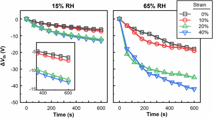
Vth shift as a function of time the bias-stress is applied. The measurements were performed under the different relative humidities of the surrounding atmosphere; 15% RH (left) and 65% RH (right).
The magnitude of ΔVth increased (Vth shifted to more negative values) with increasing application period of the bias-stress. The rate of the Vth shift was faster for the device with a larger strain on the IDTBT film, indicating that the stretching exacerbates operational instability of the OFETs under bias-stress. Notably, the rate of the Vth shift increased abruptly as the applied strain exceeded the crack onset strain (i.e., 15% strain). This result implies that the mechanism that causes the bias-stress instability of the devices is closely related to the generation of cracks in the IDTBT film. Another important trend is that the rate of the Vth shift also depends on the relative humidity (RH) of the environment around the device. A comparison of the cases where the atmospheres around the device were at 15% RH (Fig. 3, left) and 67% RH (Fig. 3, right) reveals that the measured Vth shift was slower at 15% RH than at 67% RH. That is, the bias-stress stability of the device decreased with increasing water content of the atmosphere. This trend was observed for all of the devices, irrespective of the magnitude of the strain applied to the IDTBT film. Therefore, water molecules are expected to play a critical role in the bias-stress instability of the devices.
Analyses of charge trapping and the origin of strain-dependent bias-stress stability
To unravel the origin of strain-dependent bias-stress stability of the OFET devices, we conducted a detailed analysis of the devices’ charge trapping behavior. For the devices with an IDTBT film under different strains, the amount of trapped charge carriers within the devices was quantified after the devices were bias-stressed for 600 s. PECCS analysis was performed to quantify the trapped charge carriers. In PECCS, a series of transfer curves of an FET device are obtained during the illumination with monochromatic light. When light of a certain wavelength illuminates the device, the trapped charges within the device are photo-excited, resulting in detrapping of the trapped charges. This detrapping leads to a shift in the transfer curve and the corresponding Vth; thus,the amount of charge detrapped by the illumination can be quantified from the magnitude of the Vth shift. By repeating this measurement for various photon energies, one can obtain a PECCS spectrum, that is, the density profile of trapped charges as a function of the incident photon energy. Notably, because the monochromatic light source has a limited wavelength range, PECCS is more suitable for characterizing of deep-trapped charges than shallow-trapped charges. Further details on PECCS analysis can be found in the literatures18,19,48.
We performed PECCS measurements before and after applying bias-stress and then subtracted the density profile of trapped charges within the device before the bias-stress was applied from that of the device after bias-stress was applied. The density profile of the charges trapped only by the bias-stress was thus obtained (Fig. 4). For the devices characterized under 15% RH (Fig. 4a), the results show a greater density of trapped charges for the device with larger applied strain on the IDTBT film. Two characteristic peaks are observed in the PECCS spectra, at ~1.12 and ~1.78 eV. The presence of these characteristic peaks indicates that the mechanism of the charge trapping by the bias-stress is related to these specific energies. The mechanism of charge trapping will be discussed in detail later. Integrating the area under the spectral curve gave the total amount of trapped charges, Ntrap, which was calculated for each device and plotted as a function of the applied strain (Fig. 4b). The Ntrap increased with increasing strain, indicating that the stretching of the IDTBT film led to increased charge trapping within the device under bias-stress. In addition, the tendency for Ntrap to increase with increasing strain coincided well with the trend for the magnitude of ΔVth to increase with increasing strain, implying that the bias-stress-induced shift of the Vth is indeed caused by the trapping of charges in the IDTBT film. Notably, the rate at which Ntrap increased with increasing strain showed an abrupt increase as the strain exceeded the crack onset strain (~15% strain), consistent with the trend observed previously in the ΔVth vs. bias-stress time plot (Fig. 3). The same PECCS analysis was also performed at 65% RH (Fig. 4c, d), which gave results similar to those obtained at 15% RH, except that the density of trapped charges was much greater than in the case of 15% RH.

a, c PECCS spectra of the devices. b, d Calculated trapped charge densities (Ntraps) as a function of strain. The analysis was performed under 15% RH (a, b) or 65% RH (c, d). In (b) and (d), the magnitude of Vth shift is also plotted for comparison.
In previous studies conducted by our research group, we observed characteristic peaks in PECCS spectra of OFETs and proposed explanations of their origins9,18,19,49. Two different origins for PECCS peaks were proposed: charge trapping in the in-gap state of the organic semiconductors (Fig. 5a), and charge trapping resulting from water-induced protonation of the organic semiconductors (Fig. 5b). Both types of trapped charges can be removed (detrapped) by illumination with light of a certain wavelength, thereby generating a characteristic peak in a PECCS spectrum. In Fig. 5a, the peak is obtained when a charge carrier trapped in a localized state within the bandgap is photoexcited by the incident light and detrapped from the localized state. Therefore, the energy at which a peak occurs through this mechanism directly reflects the actual energy position of the localized state and the magnitude of the peak represents the density of states of the localized states at that energy. Consequently, the positions and shapes of the peaks obtained through this mechanism are dependent mainly on the nanostructure and morphology of the organic semiconductor film9,18,19. However, in Fig. 5b, the peak is not derived from charges trapped in the semiconductor’s localized state. Instead, the trapped charge originates from the protonated form of the organic semiconductor. In a recent previous study49, we showed that IDTBT can be protonated by water under the bias-stress condition, resulting in a positively charged protonated species, [H-IDTBT]+. Because of its positive charge, this species apparently acts as a trapped positive charge and contributes to the Vth shift and the bias-stress instability of the IDTBT-based OFETs. The [H-IDTBT]+ has a narrower optical gap (~1.1 eV) than IDTBT (~1.8 eV) and upon photoexcitation by the photons with energy of ~1.1 eV, it can be neutralized via charge transfer from the surrounding IDTBT to the [H-IDTBT]+ species. Therefore, this removal of trapped positive charge (i.e., the positive charge of [H-IDTBT]+) upon ~1.1 eV illumination results in a Vth shift of the OFET, which finally leads to the appearance of a peak in the PECCS spectrum at an incident photon energy of ~1.1 eV. Similarly, the photoexcitation of IDTBT adjacent to [H-IDTBT]+ by illumination with ~1.8 eV light can also lead to neutralization of the [H-IDTBT]+, thereby generating a peak at ~1.8 eV in the PECCS spectrum. Of course, because of the structural and energetic disorders in the IDTBT layer, the peaks at ~1.1 and ~1.8 eV are inhomogeneously broadened and observed over a wide range of energies, rather than having sharp and well-defined shapes and positions. The detailed mechanism of the water-induced protonation of IDTBT and consequent charge trapping, as well as details of its effects on the occurrence of peaks in the PECCS spectrum and the bias-stress stability of the OFET can be found in our previous work49.

a Charge trapping by the in-gap trap states. Detrapping of the trapped charges by the illumination leads to the appearance of peaks in PECCS spectrum. b Charge trapping by water-induced protonation of IDTBT. The trapped positive charges carried by [H-IDTBT]+ are removed by illumination at certain wavelengths and generate peaks in PECCS spectrum at the corresponding photon energies (~1.1 and 1.8 eV). This mechanism is considered as the major charge trapping mechanism in this study. c Left: Vth shift of IDTBT FETs (with 0% or 40% strains on IDTBT film) under bias-stress, measured at a low temperature of 230 K. Right: PECCS spectra of IDTBT FETs (with 0% or 40% strains on IDTBT film) after applying bias-stress. The bias-stress was applied at a low temperature, 230 K.
In the present study, the peaks observed in the PECCS spectra are primarily attributed to the water-induced protonation of IDTBT and consequent charge trapping because the experimental conditions and results of the PECCS analysis in the present study are mostly the same as those in our previous study on water-induced charge trapping in IDTBT OFETs49. The characteristic peaks in the PECCS spectra recorded in the present study were located at ~1.1 and ~1.8 eV, consistent with peaks originating from the water-induced protonated species [H-IDTBT]+. In addition, the occurrence of these peaks was greatly suppressed (and, thus, the Vth shift of the devices was greatly reduced) when the devices were bias-stressed at a low temperature of 230 K (Fig. 5c); this phenomenon is also strong evidence for the charge trapping by water-induced protonation of IDTBT, as we demonstrated in our previous study49. Additional evidence is the RH dependence of the PECCS spectra and bias-stress stability of the devices, which showed a greater density of trapped charges and poorer bias-stress stability of OFETs in the atmosphere with 65% RH compared with those of OFETs in the atmosphere with 15% RH (Fig. 4). This dependence obviously shows that the charge-trapping mechanism is closely related to the content of water around the device under bias-stress. These experimental evidences strongly support that the charge trapping in the devices in this study originated mainly from the water-induced protonation of IDTBT.
On the basis of this interpretation, the more severe charge trapping and diminished bias-stress stability of the device with larger strain on the IDTBT film compared with those of the device with smaller strain on the IDTBT film are likely to result from greater water uptake in the device with larger strain. The abrupt increase in Ntrap as the strain increases beyond the crack onset strain (Fig. 4c, d) can be explained by the increased penetration of water molecules from the surrounding atmosphere into the IDTBT film. That is, as more cracks formed and propagated, a larger interfacial area was formed between the IDTBT and the atmosphere, enabling water molecules in the atmosphere to contact and penetrate into the IDTBT film. In addition, Fig. 4c, d shows that the Ntrap increases abruptly near the crack onset strain and then the slope is diminished as the strain is increased further; this trend is consistent with that observed in the crack density vs. strain plot in Supplementary Fig. 2. This similarity supports our speculation that the generation of cracks provides more opportunities for water molecules to penetrate into the IDTBT film and adversely affect the bias-stress stability of the device.
The generation of nanoscale cavities within the IDTBT film, as well as the decrease in the films’ crystallinity by the stretching can also be another source of the increased penetration of water molecules and consequent increased charge trapping under bias-stress. It is knwon that at low temperatures below the glass-transition temperature, the polymer chain motion in the amorphous region is restricted; thus, small cavities form even at a very small strain. Increasing strain leads to separation of the crystalline region into smaller crystallites, along with extension of the cavities50,51. In our GIXD results, we observed a mild decrease in the DoC of the IDTBT film upon stretching in the low-strain region below the crack onset strain, followed by a considerable decrease in the DoC after the crack onset strain (Fig. 2c). Therefore, stretching the IDTBT film would generate nanoscale cavities within the stretched film, and the population and size of the cavities would increase as the film is stretched and its DoC is decreased further. Because the increase in vacancies within a polymer film leads to an increase in permeability of gas molecules through the film in general52, the generation of nanoscale cavities inside the stretched IDTBT film likely increases the permeability of water molecules, eventually leading to the generation of a greater number of protonated IDTBT molecules under the bias-stress condition. The mild increase in Ntrap as a result of strains smaller than the crack onset strain (Fig. 4c, d) despite the generation of cracks in this strain range can be well explained by this mechanism.
We speculate that the strain-induced changes in polymer chain conformation and polymer chain alignment are not likely the major origin of strain-dependent charge trapping and bias-stress stability of the IDTBT FETs. As previously discussed, the IDTBT films did not show a noticeable change in the average distribution of dihedral angles of the polymer backbone throughout the investigated strain range, as revealed in our Raman spectroscopic analysis (Figs. 2e, f, and S5). In addition, our DFT calculation results show that the highest occupied molecular orbital (HOMO) energy level of IDTBT does not substantially vary with θIDT-BT, exhibiting only a small change of ~0.07 eV during the change of θIDT-BT from 0° to 30° (Supplementary Fig. 7). These results suggest that the density of states of the HOMO in the IDTBT film would not considerably change even under strain. Thus, the strain-induced structural changes in the IDTBT films are expected to cause negligible change in the energetic disorder of the film and contributed minorly to the strain-dependent bias-stability of the FET devices.
In summary, we performed PECCS analysis to investigate the charge-trapping behavior within OFETs based on IDTBT films with different strains. Charge trapping in these devices originates primarily from the protonation of IDTBT by water molecules incorporated within the film under the bias-stress condition, supported by the characteristic features of PECCS spectra (e.g., spectral shapes and their temperature dependence) and the RH dependence of the PECCS and bias-stress stability results. The greater charge trapping and poorer bias-stress instability of the device under higher strain compared with those of the device under lower strain is attributed to greater water content within the IDTBT film under higher strain. The generation of nanocavities and cracks is considered the major cause of the greater incorporated water content within the IDTBT films under higher strain. The mechanisms of water penetration into the stretched IDTBT films are illustrated in Fig. 6. Because the density of localized states in IDTBT was not expected to substantially vary between the devices, charge trapping by localized states was not considered to be the main factor affecting the strain dependence of the bias-stability of the devices.

Water content within IDTBT film increases with increasing strain. For strains smaller than the crack onset strain, nanoscale cavities are generated within the film and their population and size increase with the strain, which is accompanied by mild increase in water content within the film. For strains greater than the crack onset strain, cracks are generated and penetration of water into the IDTBT film increases abruptly.
Suppression of strain-dependent bias-stress stability by passivating the OFETs
To confirm our hypotheses related to the water-induced charge trapping and strain-dependence of the bias-stress stability of the OFETs, we investigated the charge trapping and bias-stress stability of OFETs in the absence (minimized content) of water molecules. To minimize the penetration of water molecules into the IDTBT layer, we thoroughly passivated the OFETs by depositing a combination of passivation layers. Parylene AF, Parylene C, CYTOP, and Al were used as the materials for the passivation layers. These materials exhibit low water vapor transmission rates (WVTRs): 0.22, 0.08, 0.1, and 0.3 g mm m2 day−1 for Parylene AF53, Parylene C53, CYTOP54, and Al55, respectively. Thus, the combination of these materials is expected to effectively block the penetration of water molecules into the IDTBT film. In particular, the bilayer structure of Parylene C/Parylene AF has been reported to provide a pinhole-free passivation layer with a low WVTR and low water absorption, because of its chemically stable and hydrophobic nature56,57,58. CYTOP was used to block the penetration of water molecules as well as to prevent the undesired slow-polarization effect of the Parylene C layer, which affect device operation54,59. Before passivation, the OFET devices were stored for a week with CaCl2, a moisture absorbent, in a glove box filled with N2 to remove residual water within the device. The full structure of the passivated OFET device is shown in Fig. 7a; details of the passivation process are provided in the Methods section. It should be noted that the passivation was done after the complete fabrication of the OFET devices with different strains to ensure that the strained film structures were unaffected by the passivation process.

a Device structure of passivated IDTBT FETs. b Vth shift of passivated devices under bias-stress. c PECCS spectra of the passivated FET devices after applying bias-stress.
A remarkable improvement of bias-stress stability was observed for the passivated devices (Fig. 7b). Under the atmosphere with 15% RH, the passivated devices exhibited only a small-magnitude Vth shift, (<1 V), even after a bias-stress was applied for 2000 s. In addition, the strain dependence of the bias-stress stability almost disappeared: nearly the same |ΔVth| were observed changes for the device without strain on the IDTBT film and the device with 40% strain on the IDTBT film. The PECCS spectra of these devices after the bias-stress was applied were nearly identical, and the characteristic peaks from water-induced charge trapping by protonated IDTBT ([H-IDTBT]+) were greatly suppressed, showing a negligible peak at ~1.1 eV (Fig. 7c). These results—the dramatic suppression of charge trapping and bias-stress instability in the absence of water molecules and the disappearance of strain-dependence of bias-stress stability in the absence of water molecules—strongly support our conclusions about the charge trapping mechanism and the origin of the strain-dependence of the bias-stress stability of the IDTBT OFETs. Moreover, the results suggest that the bias-stress stability of stretchable OFETs can be dramatically improved by preventing the penetration of water molecules into the devices(e.g., by thoroughly passivating the stretchable OFETs, as done in this study), irrespective of the strain applied to the devices.
Discussion
In this study, we systematically investigated the origin of strain-induced bias-stress instability of OFETs and proposed an effective method to dramatically improve the stability. We achieved these by performing comparative structural and electrical analyses on IDTBT films under different strains, together with analyses of films under different RH conditions of the surrounding atmosphere. In particular, PECCS analysis of the strained IDTBT-based OFETs played a critical role in revealing the origin of the charge trapping and strain-dependent bias-stress instability of the OFETs, by providing quantitative information—specifically, the amount of trapped charges as well as the energy of photons that was relevant to the detrapping mechanism of trapped charges within the IDTBT films.
The results showed that the bias-stress instability of the OFETs mainly arose from the trapping of positive charges within the IDTBT film as a result of water-induced protonation of the IDTBT. The charge trapping became more severe when the IDTBT film was stretched because the water content within the IDTBT film became greater when the film was stretched; as a result, the bias-stress stability of the IDTBT-based OFET deteriorated when the IDTBT film was stretched. The water content within the IDTBT film increased with increasing strain because the increase in strain was accompanied by the generation of nanoscale cavities and the formation of cracks in the film. The generation of cavities and cracks by strain provided more chances for water molecules to be incorporated into the IDTBT film, resulting in an increase of the water content within the film. When the applied strain exceeded the crack onset strain, the charge trapping and the bias-stress instability of the device abruptly increased, indicating that the cracking of the polymer film is particularly detrimental to the stability of the OFETs. On the basis of these findings, we proposed that the exclusion of water molecules during the stretching and operating of the OFETs by thoroughly passivating them can improve their bias-stress stability. Indeed, the passivated devices showed dramatically improved bias-stress stability and no dependence of bias-stress stability on the strain applied to the IDTBT film. This result further corroborated our findings related to the origin of the bias-stress instability and its strain-dependence.
Although the findings of this study are primarily based on the model conjugated polymer IDTBT, we believe that the conclusions drawn in this study are relevant not only to IDTBT but also to other p-type conjugated polymers. For instance, we have confirmed in our previous study that the same water-induced charge deep-trapping mechanism, via protonation of conjugated polymers, is also applicable to another p-type conjugated polymer, poly[2,5-(2-octyldodecyl)−3,6-diketopyrrolopyrrole-alt-5,5-(2,5-di(thien-2-yl)thieno[3,2-b]thiophene)] (DPP-DTT)49, which exhibits a significantly different crystalline nature compared to IDTBT. The deformation of conjugated polymer films through stretching is likely to enhance the penetration of water molecules into the films, irrespective of the detailed molecular structure of the polymer. Therefore, as long as protonation-induced charge trapping remains the primary factor contributing to bias-stress instability, its dependence on strain will follow the same rationale presented in this study.
We believe that this study sheds light on the understanding of charge trapping mechanism in stretchable OFETs and on the effects of stretching on the operational stability of OFETs; these effects have not been intensively investigated in previous studies. In addition, our results demonstrate that the stretching-induced bias-stress instability can be eliminated almost completely by passivating the devices, providing important insights for the development and commercialization of future bias-stable stretchable OFETs.
Methods
Materials
IDTBT (P3200 (MW/Mn = 180k/80k)) was purchased from Derthon Optoelectronic Materials Co., Ltd. PDMS (Sylgard 184) was purchased from Dow Corning with curing agents. Poly(ethylene naphthalene) (PEN) was obtained from Teijin Dupont Films.
Film preparation
Film preparation (excluding the first and second transfer processes) was conducted in an N2 glovebox to ensure reproducibility. The polymer semiconductor was dissolved in chloroform (5 mg mL−1) and stirred for at least 5 h (at 40 °C) before being spin-coated onto a heavily n-doped Si substrate with SiO2 (thickness = 3000 Å), pre-modified with an ODTS self-assembled monolayer, yielding ~30 nm thick semiconductor thin films. After spin coating, the thin film was annealed at 90 °C for 1 h.
Film transfer methods
To obtain a first-transferred polymer semiconductor, a thin film of polymer semiconductor was transferred onto a 30 µm thick PDMS supporting layer (precursor to cross-linker ratio of 10:1, cured at 60 °C overnight) using the film-on-elastomer method2. Using a custom-built stretching jig, the polymer films on PDMS were subsequently stretched to achieve the desired strain. Then, to obtain polymer semiconductor films with a desired strain on a Si substrate, the second-transfer method was adapted2. The heavily n-doped Si with SiO2 (thickness = 3000 Å) or the glass substrate was pre-cleaned using a series of solvents (Extran, deionized water, acetone, and isopropanol) for 10 min each. The substrates were then dried using N2 blowing and pre-treated with O2 reactive-ion-etching (Femto Science, VITA). The first-transferred polymer semiconductor, with the desired strain, was brought into intimate contact with the Si or glass substrate. The PDMS support was then gently and slowly delaminated, leaving the transferred semiconductor on the SiO2 surface or on the glass substrate.
Device fabrication
Bottom-gate top-contact OFETs were fabricated in a N2-filled glove box with less than 0.3 ppm of H2O or O2. Au gate electrodes (33 nm) were thermally evaporated onto the PEN substrates. A dielectric layer of polystyrene was prepared by spin coating the dielectric solution (9 wt% solution in PGMEA:cyclopentanone (9:1)) and subsequently annealed at 90 °C for 1 h to yield a dielectric layer ~ 1 μm thick. Polymer semiconductor films stretched to various strains were transferred onto the dielectric layer through the second transfer process as described in the Results section. By using thermal evaporation, the Au source and drain electrodes (33 nm) were deposited onto the semiconductor films through a shadow mask. The channel length and width were 100 μm and 1 mm, respectively.
Passivation
The fabrication of IDTBT-based OFET devices and the subsequent CYTOP spin-coating step were conducted in a nitrogen glove box with less than 0.3 ppm of H2O or O2. The fabrication process of the OFETs adhered to a previously described method. After the fabrication, the devices were stored in the glove box for a week with a CaCl2 desiccant, ensuring no contact between the OFETs and the desiccant. A CYTOP layer (7 µm) was spin-coated onto the OFET devices. Subsequently, the devices were dried for 1 h at 25 °C, then further dried on a 40 °C hot plate for 2 h, before being transferred to a vacuum chamber for 2 days. Using a Parylene Coater (OBT-PC300, Obangtechnology), Parylene C and AF layers were deposited via chemical vapor deposition while maintaining the temperature of the devices at near-room temperature. Before each Parylene deposition process, the devices were preconditioned in the parylene vacuum chamber for at least 4 h with a CaCl2 desiccant. Initially, layers of Parylene C (20 µm), Aluminum (400 nm), Parylene C (20 µm), and Parylene AF (20 µm) were sequentially deposited on the bottom side of the devices. Subsequently, layers of Parylene C (20 µm) and Parylene AF (20 µm) were deposited on the top side of the devices.
Morphological characterizations
Crack density and area was measured from the optical microscope images of strained films using an image processing software ImageJ. The crack density was defined by the number of cracks per unit length along the strain direction, as defined earlier in the Result section. Multiple lines and areas were selected and used for the calculation to give average values. AFM measurements of the surface morphology were obtained at the second transferred films using a Bruker NanoScope V. A backscatter configuration with a 30× objective lens and 538 nm laser excitation in Witec Alpha 300 was adapted to measure Raman spectra. The measurements were performed after stabilization of the laser. To ensure consistent results, the laser power and acquisition time were optimized and kept constant across all measurements. UV–vis spectra were measured on an Agilent Cary 5000 spectrophotometer for first transferred polymer semiconductors at the desired tensile strain. 2D-GIXD was performed with the second transferred films at the 3C or the 9A beamlines with a critical incident angle of each sample (a photon energy of 11.6 keV) at the Pohang Accelerator Laboratory (PAL).
Electrical characterizations
Electrical measurements were carried out using a custom-built probe station (MS-TECH) equipped with temperature controllers and an environment control chamber (N2, vacuum, and humid atmosphere). A Keithley 4200 semiconductor parameter analyzer was employed to measure bias instability. The Vth values were determined in the saturation regime, and ΔVth was derived after prolonged (600 s) bias stress (bias stress conditions: VGS and VDS = –60 V) by comparing it to the initial Vth values. To ensure reliable temperature or environmental dependency, the target temperature or environment was maintained for 30 min, allowing the OFETs to reach thermal or environmental equilibrium before conducting the measurements.
Photo-excited charge collection spectroscopy (PECCS)
To conduct PECCS measurements, the custom-built probe station (MS-TECH) described in the electrical characterizations section was further connected to a 500 W Hg (Xe) arc lamp light source and a grating monochromator with a 300–2000 nm spectral range. An optical fiber with a 1000 μm core diameter served as an optical probe to guide photons onto the active channel area of the OFETs. The light source had a high spectral irradiance exceeding 20 mW m–2 nm–1 over the entire wavelength range used in the PECCS measurement, which guaranteed a sufficient photon flux required for the complete de-trapping of trapped charges. A Keithley 4200 semiconductor parameter analyzer was employed to measure the transfer characteristics under the monochromatic light and in dark conditions, in order to compare the shifts in the Vth of the OFETs. PECCS measurements were performed before and after applying bias stress.


Responses