Stretchable nanogenerator with micro-nano hierarchical interfaces for self-powered biometric authentication

Introduction
The rapid development and widespread popularity of the Internet of Things (IoT)1,2,3 have promoted the advancement of wearable electronics in terms of miniaturization, multifunctionality, smart integration, and several excellent physical properties in wearable devices, such as flexibility, stretchability, and surface adaptability4,5,6,7,8,9. However, there are several crucial challenges in the progress of wearable electronics, particularly multifunction integration, and heterogeneous surface integration. In the case of these two key demands, one promising solution involves developing stretchable biomechanical microenergy harvesters10,11,12 used to convert ubiquitous biomechanical microenergy from human activities to sustainable and reliable electricity for powering microelectronics, as well as self-powered sensing.
Three typical biomechanical microenergy harvesters have been reported in the last few decades: triboelectric nanogenerators (TENGs)13,14,15, piezoelectric nanogenerators (PENGs)16,17,18, and electromagnetic generators (EMGs)19,20. These have been proven to be attractive biomechanical microenergy harvesters and/or self-powered sensors owing to the unique correlation between the electrical outputs and mechanical inputs. Different types of biomechanical microenergy harvesters have inherent configurations, particularly differing in their stretchable strategies, which endow them with extensive abilities, mechanical properties, electrical performance, and wearable applications. For instance, traditional electromagnetic generators exhibit outstanding output performance, however, their inherent properties, such as heavyweight and bulky volume owing to the key components of bulk magnets and coils, render it difficult to satisfy wearable requirements. In recent years, stretchable electromagnetic generators have been proposed by miniaturizing magnets and coils, using commercial flexible coils, or developing stretchable coils and ferromagnetic materials, which inevitably and significantly reduce their electrical outputs. Stretchable strategies, such as using piezoelectric polymer (e.g., polyvinylidene difluoride (PVDF)) or compositing solid piezoelectric particles (e.g., lead zirconate titanate (PZT), and barium titanate (BaTiO3)) with a polymer matrix (e.g., polydimethylsiloxane (PDMS), and silicone rubber (SR)), can result in low electrical outputs of stretchable PENGs. In comparison, the advantages of a relatively larger range of material selection and relatively high outputs facilitate stretchable TENGs in realizing a better trade-off between outputs and mechanical demands and are more attractive in the field of biomechanical microenergy harvesting.
The essential challenge of stretchable triboelectric nanogenerators is to endow their functional components (such as conductive electrodes and triboelectric materials) with good extensive ability, and ultimately achieve scalable heterogeneous integration of the discrete functional components by advanced micro-nano integrated manufacturing21,22,23,24,25. In this study, a fully stretchable TENG (STENG) was developed. The triboelectric pair was composed of a micro-pyramidal polydimethylsiloxane (PDMS) film with inherent stretchability and a thermoplastic polyurethane (TPU) nanofiber film with good deformability. The unique configuration of micro-nano hierarchical interfaces realized by soft lithography or electrospinning processes endowed the device with an enhanced output. Highly conductive silver nanowires (AgNW), another key component of electrodes, were introduced to form conductive networks, combined with a stretchable strategy of polymer infiltration. Consequently, stretchable silver nanowire/silicone rubber (AgNW/SR) composite electrodes were successfully obtained, and the proposed STENG with good deformability was constructed. Thus, the proposed STENG exhibited the typical configuration of a contact-separation mode-based TENG. Once the mechanical input triggered the occurrence of the contact-separation process on the triboelectric interfaces, the STENG generated electricity based on the coupling effect of triboelectrification and electrostatic induction. To evaluate the output performance of the STENG quantitatively, the mechanical input was fixed at a vertical force of 6 Hz. Consequently, the developed STENG generated an output voltage, output current, and maximum output power of 250 V, 260 μA, and 103 μW, respectively, which were proven for powering low-power-consumption microelectronics with a power management circuit (PMM). In addition, according to the quantitative correlation between the STENG outputs and mechanical inputs, the STENG can be used as a multifunctional self-powered sensor for personal activity monitoring, i.e., force, frequency, and bending sensing. It provides feasibility for the attractive application of biometric authentication26,27,28. In this study, we developed a keystroke recognition array based on the STENG. Using a support vector machine (SVM)5,29,30, the STENG array successfully achieved user identification based on the difference in the biometric features of personal activities (e.g., typing force, frequency) with a high accuracy of 93.21%. Besides, the intruders could be distinguished from all users, with an accuracy of 81.50%. This revealed the promising potential of the developed STENG for self-powered wearable applications.
Results and Discussion
Morphology of the STENG
Figure 1a schematically illustrates the structural design of the developed STENG, adopting the typical design of contact-separation-mode TENG. It can be divided into three parts, i.e., top, middle (i.e., silicone rubber spacers), and bottom. The top part comprised one friction layer of micro-pyramidal PDMS, a silver nanowire/silicone rubber (AgNW/SR) electrode (T.), and a silicone rubber layer (T.). The bottom part comprised the other friction layer of the TPU nanofiber, solid TPU substrate, AgNW/SR electrode (B.), and silicone rubber layer (B.). The middle silicone rubber spacers were used to provide space for the relative movement of the friction pair of the contact-separation mode STENG. Figure 1b shows a photograph of the fabricated STENG. It had 200% stretchability (Supplementary Fig. 1), exhibiting a good mechanical capability for wearable applications.

a The structural configuration of the STENG, in which the micro-nano hierarchical interfaces were described in the enlarged view. (b) Photograph of the STENG (Scale bar: 5 mm). (c–f) Morphologies of the triboelectric pair, i.e., (c,e) micro-pyramidal PDMS (Scale bar: 40 μm) and (d,f) all-nanofiber TPU (Scale bar:4 μm). (g) Surface morphology of silver nanowire (AgNW) conductive network layer (Scale bar: 400 nm).
Figure 1c, e, and d, f show the morphology of the fabricated micro-nano hierarchical interfaces, i.e., micro-pyramid PDMS and TPU nanofiber, respectively. The orange color shown in Fig. 1c, d was the result of placing copper foil on the bottom of the two films. The micro-pyramid structures on the PDMS surface are presented in Fig. 1e, in which the side length of each micro-pyramid is 20 μm, and the spacing between adjacent micro-pyramid units is 4 μm. And the nano-fibered TPU is shown in Fig. 1f. Notably, the TPU nanofiber was an optimized electrospun TPU (3-2), as shown in Supplementary Fig. 2. Liquid TPU (m-n) means the liquid TPU consists of pure TPU solution and TPU toughing agent solution in a weight ratio of m:n. Photographs and surface morphologies of electrospun TPU films based on different liquid TPU concentrations, i.e., TPU (1-0) (pure TPU), TPU (2-1), and TPU (3-2), are shown in Supplementary Fig. 2a, b, and c, respectively. The low viscosity of TPU (1-0) and TPU (2-1) resulted in insufficient entanglement of the solution molecular chains, rendering it difficult to balance the stretching of the electric field force. Thus, the bead phenomenon existed in the electrospun TPU (1-0) and electrospun TPU (2-1). Herein, the problem was solved by increasing the TPU toughening agent concentration to 40% (i.e., electrospun TPU (3-2)). The all-nanofiber TPU was successfully obtained, as shown in Supplementary Fig. 2c. Figure 1g shows another key component of STENG, i.e., AgNW networks, and the stretchable AgNW/silicone rubber electrodes could be obtained by infiltrating liquid silicone rubber on the AgNW networks.
Working principle of the STENG
Figure 2 schematically illustrates the power generation principle of the developed STENG in the contact-separation working mode. This includes four essential processes. Initially, the STENG was in an electrostatically neutral state. When an external force caused the triboelectric pair of micro-pyramidal PDMS and all-nanofiber electrospun TPU to come in close contact, the two micro-nano hierarchical interfaces generated equivalent numbers of triboelectric charges with opposite polarities (Fig. 2a) owing to the triboelectrification effect. Given that TPU is more triboelectrically positive than PDMS31, the micro-pyramidal PDMS surface was negatively charged, and the all-nanofiber electrospun TPU surface was positively charged.
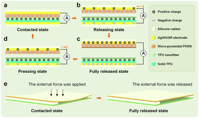
a In the initial state, the external force causes the triboelectric pair of micro-pyramidal PDMS and all-nanofiber electrospun TPU to come in contact. Based on the triboelectrification, negative and positive charges are induced on the two surfaces, respectively. b, c As the external force releases, the micro-pyramidal PDMS gradually leaves the all-nanofiber electrospun TPU, the current is induced in the external circuit resulting from the electrostatic induction. c, d When the external force is applied again, the reversed current is induced in the external circuit. It demonstrates the capability of the STENG to convert mechanical microenergy into electricity. e Illustration of two key working states of the STENG, i.e., contacted state and fully released state.
When an external force was released, the PDMS (as well as the top part of the STENG) left the TPU and gradually rebounded to the initial state (i.e., the steps in Fig. 2a–c). Thus, an internal electrical potential can be established between the two electrodes. The unbalanced positive/negative charges caused the accumulation of negative/positive charges on the bottom/top AgNW/SR electrodes due to electrostatic induction. Consequently, the accumulated charges flowed from the bottom electrode to the top electrode through an external load, and a current pulse was generated (Fig. 2b). As the micro-pyramidal PDMS moved toward the electrospun TPU again (i.e., the steps of Fig. 2a, c, d), the charges on the top electrode were driven to flow back to the bottom electrode via the load, and an opposite current was obtained (Fig. 2d). Therefore, during the release and pressing cycles of the triboelectric pair, electrons were induced to flow between the top and bottom electrodes to form currents. To clearly illustrate the process, the two key working states of the contacted and fully released states of the STENG are schematically depicted in Fig. 2e.
Electrical performance of STENG
Given that the specific surface area is one of the essential factors studied to enhance the electrical outputs of triboelectric nanogenerators (TENGs)32,33,34, especially stretchable TENGs, a contacted-separation mode TENG model (Supplementary Fig. 3) was built to study the effect of the proposed micro-nano hierarchical interfaces, i.e., micro-pyramid PDMS and nano-fibered TPU on the STENG output. Figure 3a schematically illustrates the working status of the device using different structures of PDMS and TPU, including smooth PDMS (S-PDMS) & solid TPU, S-PDMS & TPU nanofiber, micro-pyramid PDMS (P-PDMS) & solid TPU, and P-PDMS & TPU nano-fiber. Both nano-fibered TPU and micro-pyramid PDMS (Fig. 3b) could provide a larger specific surface area than the non-structured friction pair,which endows the P-PDMS & TPU nano-fiber based-STENG model with the higest output, the peak-to-peak voltage was increased by 1.27 times that of the non-structured friction pair, as shown in Fig. 3c.
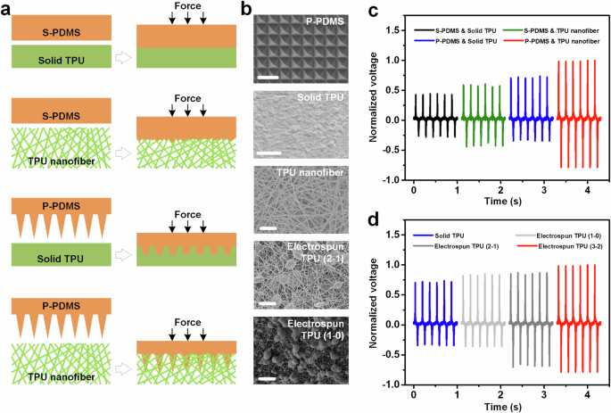
a Comparison in the contracted state of triboelectric pair (i.e., PDMS & TPU) based on different surface morphology, including smooth PDMS (S-PDMS) & solid TPU, S-PDMS & TPU nanofiber, micro-pyramid PDMS (P-PDMS) & solid TPU, P-PDMS & TPU nanofiber. b Surface morphology of P-PDMS (Scale bar: 40 μm), solid TPU (Scale bar: 10 μm), TPU nanofiber (i.e., electrospun TPU (3-2), scale bar: 10 μm), electrospun TPU (2-1) (Scale bar: 10 μm), and electrospun TPU (1-0) (Scale bar: 10 μm). c Normalized positive voltage outputs of the TENG model based on different structures of triboelectric pair. d Normalized positive voltage outputs of the TENG model based on different TPU friction layers.
Besides, the influence of different structured TPU (i.e., solid TPU, electrospun TPU (1-0), electrospun TPU (2-1), and electrospun TPU (3-2)) on the output of the device was studied. In this case, the other friction layer was P-PDMS. As depicted in Fig. 3d, the electrospun TPU films provided higher outputs for the TENG model than the solid TPU film because of the larger contact area between the electrospun TPU and P-PDMS. It is worth mentioning that the uneven surface of the solid TPU film was caused by the irregular surface of the aluminum mold. In addition, the three different electrospun TPUs exhibited unique micro/nano structures, resulting in a difference in the contact area with the micro-pyramidal PDMS, and thereby in the voltage outputs of the TENG model. Consequently, electrospun TPU (3-2) (i.e., TPU nanofiber) could endow the model with the highest voltage output among the three different electrospun TPU, further proving that electrospun TPU (3-2) was optimal for the STENG.
Figure 4 shows the electrical outputs of the fabricated STENG under continuous force at a fixed frequency of 6 Hz from the vibration platform. The positive peak output voltage and the positive peak output current of the device were approximately 250 V and 260 μA, respectively, as depicted in Fig. 4a, b, respectively. In addition, the output power of the STENG was evaluated by connecting the device with external loading resistors with values of 0.1–100 MΩ in parallel to measure the output peak voltage of the resistor and thereby its instantaneous output power. Figure 4c shows the output peak power of the STENG. It had a high internal resistance of approximately 30 MΩ, at which the maximum output peak power reached 103 μW. Considering that the effective area of the device was 2 cm × 3 cm; thus, the instantaneous power density of the device was 17.2 μW/cm2. The transferred charges of STENG in a working cycle were evaluated as 35 nC by charging a 10 nF capacitor connecting with STENG via a full-wave rectifier bridge (i.e., the inset circuit of Fig. 4d). Notably, the sub-peak signal shown in Fig. 4d resulted from the unique electrical output of TENGs, i.e., alternating pulse electrical outputs, as shown in Fig. 4a, b. As a result, the capacitor was sequentially charged by the positive and negative pulse outputs of a working cycle, which caused the formation of the sub-peak signal.
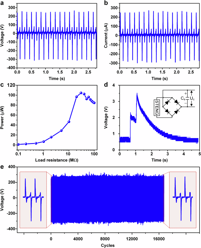
a Output voltage. b Output current. c Output power. d The transferred charges in a working cycle. e The fatigue test of the STENG was performed by evaluating the voltage variation trend during 16500 consecutive operations.
Moreover, a fatigue test was performed on the STENG, as shown in Fig. 4e. After 16,500 working cycles, the voltage output of STENG only had slight dynamic changes, meanwhile, the bonding between layer-by-layer functional components was maintained (Supplementary Fig. 4), which proved the good durability of STENG. Overall, the developed STENG had a remarkable microenergy harvesting capability, exhibiting an attractive potential for microelectronics powering.
Integrated microenergy powering and multifunctional sensing of the STENG
To realize the promising application of the STENG for microelectronic powering, the tremendous impedance mismatch between the STENG (approximately 30 MΩ) and the microenergy storage unit (usually low to ohmic level) must be addressed to achieve effective energy delivery from the STENG to the energy storage unit (i.e., capacitors). This study used a transistor-controlled power management circuit (TC-PMM, Supplementary Fig. 5)35 proposed in a previous study, which improved the energy-delivery capability of the device, as shown in Fig. 5a. Using the TC-PMM, the developed STENG could charge a 10 μF-capacitor to 4.5 V within 60 s, which is 2.25 times that without TC-PMM. As a practical application for microenergy supply, the developed STENG successfully drove a commercial hygrothermograph by charging a 10 μF-capacitor to 11 V within 4 min, as shown in Fig. 5b, thus demonstrating the feasibility of the device for powering microelectronics.
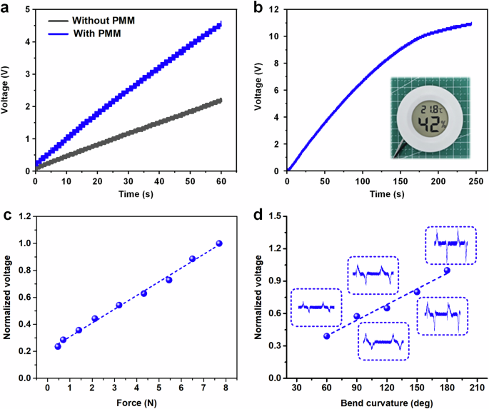
a, b Microelectronics powering. a Charging ability of the STENG without/with the help of a power management circuit (PMM). b Demonstration of the STENG to power a low-power-consumption microelectronic. c, d Self-powered sensing: c Responsive behavior of STENG outputs to force of the external excitation. d Normalized positive outputs of STENG at different bend curvatures.
Figure 5c quantitively evaluates the relationship of the STENG output to the force of the mechanical input. The STENG output increased almost linearly with increasing force, indicating the feasibility of the STENG for self-powered force sensing. The relationship between STENG output and mechanical input was quantitively studied. Supplementary Fig. 6 shows that when the applied frequency of the external force increased from 1 Hz to 7 Hz with an increasing step of 1 Hz, the voltage output of the STENG gradually increased. With a frequency increase greater than 7 Hz (i.e., the frequency range of 8–10 Hz), the voltage output of the STENG decreased. This was attributed to the under-recovery effect of the STENG because the excessively short time of the applied force at a relatively high frequency did not allow it to completely recover to its original state. Furthermore, in combination with practical wearable application scenarios wherein the frequency of human activities was approximately ~6 Hz (within the frequency range of ~7 Hz), the voltage output of STENG was almost linearly positive with the frequency of mechanical input, indicating the feasibility of self-powered frequency sensing. With the merit of the good mechanical deformation ability of the STENG, it could work under cyclic bend-release processes. When the device was cyclically bent and released at bend curvature from 60o to 180o in a step of 30o, the positive peak voltage output of STENG increased almost linearly with increasing bend curvature, as shown in Fig. 5d, showing the potential for self-powered bend sensing.
Overall, this developed STENG successfully achieved the integration of microenergy harvesting and multifunctional self-powered sensing (i.e., force, frequency, and bend sensing), demonstrating the attractive feasibility of the STENG for microenergy supply and biometric-motion sensing applications in daily life.
Self-powered biometric authentication application of the STENG array
With the rapid development of the Internet of Everything and powerful supercomputers, user security is an essential issue in modern society, whether in military or civilian scenarios. To protect against potential security threats and identity theft, biometric identification technology28,36,37 has been proposed in recent years. Since each individual has unique biometric characteristics, it can make up for the defects of traditional identity authentication (e.g., static password, short message system password, and dynamic password) based on cryptography, and ensure the dual authentication of digital identity and physical identity of users in the network environment. Potentially, TENGs have been proved to be a promising technology for safe identification in combination with biometrics, due to their unique quantitative relationship between the TENG output and the mechanical input26,38,39,40.
With the merits of self-powered force and frequency sensing capabilities of the STENG. Herein, a keystroke dynamic recognition array based on the STENG for self-powered biometric authentication was developed. As shown in Fig. 6a, nine STENG keys were arranged in three rows and three columns to form a wearable stretchable triboelectric keyboard (STENG array). Figure 6a illustrates an explosive view of the STENG array to represent its configuration, including the silicone rubber layer (B.), arrayed AgNW/SR electrodes (B.), solid TPU substrate, TPU nanofiber; and the arrayed top part of the STENG composed of the micro-pyramidal PDMS, AgNW/SR composite electrodes (T.), and silicone rubber layers. In addition, four silicon rubber spacers were built to construct the developed 3 × 3 STENG array.
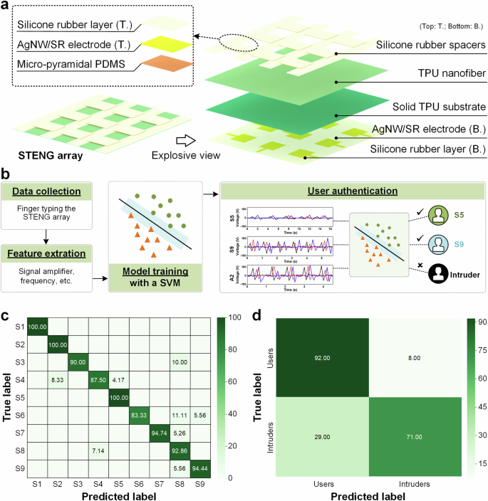
a Structural design of the developed stretchable keyboard. b Four key processes for realizing the function of self-powered biometric authentication: data collection, feature extraction, model training with a support vector machine (SVM), and user authentication based on the built model, including intruders and different users. c Confusion matrix for all night users who were sampled in the model, demonstrating a high classification accuracy of 93.21%. d Confusion matrix for users and intruders, showing a identification accuracy of 81.50%.
Figure 6b illustrates four key processes for realizing the application of self-powered biometric authentication. The first step involved collecting personal data using the STENG array. The STENG array was used to convert the typing motions of different subjects into electrical signals. Before the test, all the users were instructed regarding the data-collecting process. The users were asked to type their fingers 120 times in the STENG array in a 2-5-8 sequence. The collected 85% of the data were used for the training process and 15% of the data were used for the identification process. The second step was the feature extraction of the collected data from all the users. Supplementary Figs. 7 and 8 show the collected data of all users who were sampled in the model, and the intruders who were not sampled in the model, respectively. The differences in typing force and typing time of the subjects affected the output signals, especially in amplified and frequency, and they were used for feature extraction of the output signals. The third step involved training these extracted features using an SVM to build a model for user identification.
Notably, the SVW is a machine learning algorithm that uses supervised learning models to solve linear or nonlinear classification, regression, and outlier detection problems. An optimal decision hyperplane needs to be established to maximize the distance between the two types of samples on the two sides of the plane that are closest to the plane, offering a good generalization ability for the classification problem. For multi-dimensional sample sets, the system randomly generates a hyperplane and continuously moves to classify samples until the sample points belonging to different categories in the training samples are located on both sides of the hyperplane. Recently, many hyperplanes are satisfied with the conditions, in which SVM officials found such a hyperplane while ensuring classification accuracy, maximizing the blanks on both sides of the hyperplane, thereby achieving optimal classification of nonlinearly separable samples. Besides, SVM is one of the candidates for human activity recognition as the data size is relatively small5.
The final step is using the established model to distinguish between the different users and the intruders who are not sampled in the model. Herein, all users were recognized with a high accuracy of 93.21%, as shown in Fig. 6c of the classification confusion matrix. Besides, the model could be used to identify the users and the intruders who are not sampled in the model. The same amount of data from users and intruders was used for the identification process, the identification accuracy reached 81.50%, as shown in Fig. 6d. Here, the error in users’ identification occurred inevitably. Because it’s difficult for every user to maintain a fixed force and frequency to tap the STENG array continuously, which causes the output changes of each STENG key. Besides, the Principal Component Analysis (PCA) for dimensionality reduction was performed on the feature vectors. Supplementary Fig. 9a, b show the feature visualization result of the data from all users, and the data from users and intruders in a 2D space, respectively. Both demonstrated the potential of the STENG array-based-wearable triboelectric keyboard for highly-accuracy and self-powered biometric authentication.
Overall, a novel configuration of the stretchable TENG with micro-nano hierarchical interfaces was proposed in this study. The combination of one micro-structured friction material (i.e., micro-pyramidal PDMS (P-PDMS)), and the other nano-fibered friction material (i.e., TPU nanofiber) provides an effective strategy for the output improvement of stretchable TENGs. In addition, the developed STENG achieved the multifunction integration of microenergy powering and self-powered multifunctional sensing (i.e., bend sensing, force, and frequency sensing) with high linearity, and the sensing abilities endow the device with good biometric capability. As an application, an STENG array-based wearable triboelectric keyboard was proposed. The dynamic keystroke motions of all users were identified, with a high accuracy of 93.21%. Besides, the intruders who were not sampled in the model were distinguished from users, with an accuracy of 81.50%. Both proved the remarkable self-powered biometric authentication ability of the STENG array based-keyboard device.
Methods
Preparation of solid TPU substrate and TPU nanofiber
Its excellent stretch recovery and adjustable deformability render TPU a potential candidate for the fabrication of stretchable polymers. Figure 7a<i> shows the preparation of the stretchable TPU substrate, including three steps. First, liquid TPU was prepared. It consisted of TPU powders (15wt%), and two solvents of N, N-Dimethylformamide (DMF, 56.7wt%) and Tetrahydrofuran (THF, 28.3wt%). Liquid TPU was obtained by dissolving the TPU powders in a DFM/THF mixer under magnetic stirring at room temperature for 4 h.
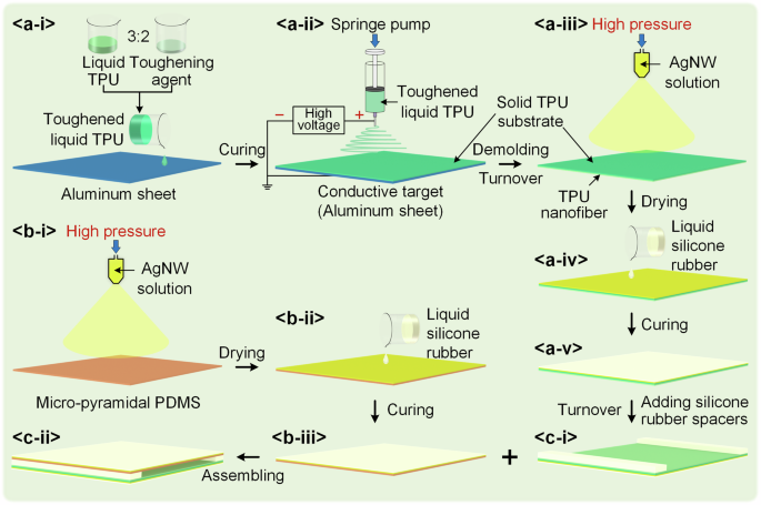
a Preparation of STENG’s bottom part with (i) solid TPU substrate, (ii) TPU nanofiber, (iii) silver nanowire (AgNW) networks, and (iv-v) AgNW/silicone rubber (SR) composite electrode with a silicone rubber layer. b Fabrication of STENG’s top part with (i-ii) AgNW networks on micro-pyramidal PDMS layer without microstructures, and (ii-iii) AgNW/SR composite electrode with a silicone rubber layer. c Assembly of the top and bottom parts with two fabricated silicone rubber spacers, and the developed STENG could be obtained.
To obtain a stretchable TPU substrate with good extensive ability and remarkable stretch recovery, a TPU toughening agent was required to improve and adjust the stretchability of the TPU film. The toughened liquid TPU was composed of the obtained liquid TPU and toughening agent in a weight ratio of 3:2. The toughening agent was prepared by dissolving solid toughening agent (33.3wt%) in DFM (66.7wt%) under magnetic stirring at 110 °C for 2 h.
Third, the preparation of stretchable TPU substrate. The toughened liquid TPU was vacuum-deformed for 30 min to remove bubbles from the solution. After the toughened liquid TPU was roller-coated onto an aluminum sheet, vacuum deformation was performed again to remove bubbles in the solution and the interface between the solution and the aluminum sheet. Then, the stretchable TPU film was obtained by curing the solution at 110 °C for 1 h. Notably, the aluminum sheet was used as a collector for the electrospinning process, and the prepared stretchable TPU film was used as the stretchable substrate for the following all-nanofiber TPU mat.
The TPU nanofiber was fabricated by electrospinning. Three parameters significantly impact the formation of all-nanofiber TPU: (i) the applied high voltage, (ii) the distance between the collector and the spinneret (i.e., the jet path), and (iii) the constant speed of 3-2TPU solution that was pushed out of a tank (i.e., a 10 mL syringe with a needle inner diameter of 0.5 mm) to a spinneret, which was optimized as 8.0 kV, 15 cm, and 0.5 mL/h, respectively. After electrospun for 4 h, the all-nanofiber TPU could be obtained on a TPU substrate. Finally, the all-nanofiber TPU with TPU substrate was obtained by peeling off it from the Al collector.
Preparation of micro-pyramidal PDMS
Soft lithography is an effective method to endow polymers (e.g., PDMS, hydrogels, and silicone rubber) with micro/nanostructures. In this study, the developed micro-pyramidal PDMS was prepared using soft lithography, realizing the replication of micro-pyramidal structures from a prepatterned silicon mold to a stretchable PDMS film. The detailed steps are summarized as follows. First, the PDMS solution was prepared by mixing the base solution and curing agent at a weight ratio of 10:1, followed by vacuum deformation for 20 min to remove bubbles from the PDMS solution. Second, the prepared PDMS solution was dispensed onto the pre-patterned silicon mold, followed by vacuum deformation for 20 min to remove bubbles in the PDMS solution and the interface between the PDMS and the silicon mold. After curing the liquid PDMS at 75 °C for 30 min, the micro-pyramidal PDMS film was obtained by peeling it off the silicon mold.
Fabrication of the developed STENG
Successive spray coating and polymer infiltration were utilized to prepare AgNW/ silicone rubber electrodes on the fabricated stretchable PDMS film and TPU substrate. First, a 2 mg/mL AgNW/ethanol solution was prepared by diluting a commercial 20 mg/mL AgNW/ethanol solution. Thereafter, AgNW networks were constructed by spray coating 5 mL 2 mg/mL AgNW/ethanol solution on the PDMS surface without micro-pyramidal structures and the solid TPU substrate without electrospun TPU, as shown in Fig. 7a<iii> and 7b<i>, respectively. The PDMS and TPU films were placed atop a 50 °C hot plate during the spray coating process, thereby realizing the evaporation of ethanol solvent for each spray.
Furthermore, the AgNW/SR composite electrodes were prepared by infiltrating liquid silicone rubber into the spacer of AgNW networks, followed by curing the liquid silicone rubber at room temperature of 4 h. Consequently, stretchable AgNW/SR electrodes were realized (Fig. 7a<iv-v> and b<ii-iii>). To provide a relative motion space between the triboelectric pair (i.e., micro-pyramidal PDMS and electrospun TPU), two rectangular silicone rubber spacers were prepared and fixed at both ends of electrospun TPU layer, as shown in Fig. 7c<i>, followed by assembling the top part of the STENG (i.e., micro-pyramidal PDMS, AgNW/SR electrode with a silicone rubber layer) with the silicone rubber spacers and the bottom part of the STENG (i.e., all-nanofiber electrospun TPU, TPU substrate, AgNW/SR electrode with a silicone rubber layer), as shown in Fig. 7c<i-ii>. Liquid silicone rubber was chosen as the bonding medium among the interfaces of the micro-pyramidal PDMS, silicone rubber spacers, and all-nanofiber electrospun TPU. After curing the interfacial silicone rubber at room temperature for 4 h, the STENG was obtained.
Materials and Measurements
Polydimethylsiloxane (PDMS, Sylgard 184), consisting of a base solution (prepolymer) and a curing agent, was purchased from Dow Corning. Silicone rubber (SR, EcoflexTM 00-30) comprised of PART A and PART B was purchased from Smooth-On. Thermoplastic polyurethane (TPU) powder was purchased from BASF, and the TPU toughening agent particle was purchased from Lubrizol. N, N-Dimethylformamide (DMF), and Tetrahydrofuran (THF) were purchased from Shanghai Aladdin Biochemical Technology. AgNW/ethanol solutions were purchased from Nanjing Xian-Feng Nanomaterial Technology (XFNANO).
The surface morphologies of the micro-pyramidal PDMS, TPU layers, AgNW network layer, and the interfacial view between the functional layer were characterized using scanning electron microscopy (SEM, JSM-6490LV, JEOL Ltd.). An electrospinning platform was built using a voltage power source to provide a positive voltage, an electric displacement platform to control the ejection speed of the polymer solution, an aluminum collector, and a 10 mL springer. A hot plate (XG-2020) was used to provide a controllable temperature for the spray coating. A spray gun was used to spray a conductive AgNW/ethanol solution. A vibration platform comprising a signal generating system (33250 A, Agilent), power amplifier, and shaker was used to provide a stable and controllable vertical force for measuring the output performance of the STENG. In addition, the output voltages were measured using a digital oscilloscope (DS2302A, RIGOL) with a 100 MΩ probe. Further, the output currents were amplified using a low-noise current preamplifier (SR570, SRS) and then measured using a digital oscilloscope (DS2302A, RIGOL) with a 100 MΩ probe. The mechanical property of STENG was evaluated by a push and pull tester ((HP-50, HANDPI) consisting of a force gauge and a displacement meter. The sensor experiments demonstrated in Fig. 6 were conducted with the approval of the university ethics committee and written informed consent was provided by all participants.


Responses