Switching on and off the spin polarization of the conduction band in antiferromagnetic bilayer transistors

Main
In antiferromagnetic conductors, spin order breaks time-reversal ((hat{T})) symmetry. However, if a time-reversal symmetry transformation followed by spatial inversion ((hat{P})) or by a translation remains a symmetry (so-called crystal time-reversal symmetry), antiferromagnets can behave as if (hat{T}) symmetry was effectively present1,2,3,4,5. These considerations are key for antiferromagnetic spintronics6,7,8,9, since the breaking of such ‘effective’ time-reversal symmetry causes physical phenomena characteristic of ferromagnets (anomalous Hall effect10,11,12,13, spin-polarized bands14,15,16,17 and so on), despite the absence of a net magnetization. Identifying bulk antiferromagnets that exhibit these phenomena requires a detailed analysis of the crystalline and magnetic structures, to determine whether (hat{T}) symmetry is effectively broken2,10. Symmetry considerations analogous to the ones just mentioned are leading to unanticipated results, such as the discovery of altermagnetic compounds3,4,13,16,17, and are responsible for the rapid development of antiferromagnetic spintronics.
It has been proposed that in some two-dimensional (2D) antiferromagnetic semiconductors18,19,20,21,22,23, spatial symmetries can be controlled experimentally enabling switching on and off at will the effect of time-reversal symmetry24,25,26,27,28. This is the case for bilayers of A-type antiferromagnetic semiconductors, in which the magnetization of one layer is equal and opposite to that of the other layer. Their low-energy conduction band is formed by spin-degenerate states residing in either one of the two layers, whose spin direction is determined by the magnetization of the corresponding layer. The conduction band therefore consists of spin-unpolarized bands, associated to spatially separated electronic states. Under a perpendicular electric displacement field (D), inversion and space-time symmetry are broken, as the interlayer electrostatic potential difference shifts states with one spin to energies lower than states with the opposite spin (Fig. 1a and Supplementary Note 1). The conduction band becomes spin-polarized, and the spin polarization can be reversed by inverting D.

a, Schematics of the low-energy band structure. An A-type antiferromagnetic bilayer hosts switchable spin-up (-down) bands, located in separate layers. The red (blue) spin-up (-down) bands represent the dispersion relation of states in the top (bottom) layer. At zero displacement field (D/ε0 = 0, top panel), the potential difference (Delta)U between the layers vanishes, and the spin-up and -down bands are degenerate. At finite (Delta)U (D/ε0 ≠ 0, middle and bottom panels), the interlayer potential difference lowers the energy of states in one layer (hence with one spin polarity) relative to the other, thereby breaking inversion ((hat{P})) and space-time ((hat{P}hat{T})) symmetry. Reversing the sign of D/ε0 lowers the energy of states located in the other layer (bottom panel), with opposite spin (Supplementary Fig. 1). b, Schematic representation of a double-gated CrPS4 bilayer transistor of the type used in this work (see Methods for fabrication details). The zoom-in panel shows a side view of the CrPS4 crystal structure (the red, blue, yellow and orange balls represent top-layer Cr, bottom-layer Cr, P and S atoms, respectively). The double-gated geometry enables independent control of the electron density (ne) and displacement field (D/ε0 = (DT + DB)/2ε0; DT (DB) is the displacement field generated by the top (bottom) gate). c, Source (S)–drain (D) current I measured in the transistor as a function of top-gate voltage VTG (transfer curve) at fixed back-gate voltage VBG = 0. d, Transfer curve measured as a function of VBG for VTG = 0. e, Colour plot of I as a function of VBG and VTG. The black (white) dotted line corresponds to a constant density (displacement) profile. Data shown in this figure were measured at VSD = 2 V and at 2 K.
Source data
The spatial separation of spin-split bands also gives control over their electronic population by using double-gate field-effect transistors (FETs) that allow tuning independently D and the accumulated charge density (ne)29,30,31,32,33. At zero electric field (D/ε0 = 0), the potential of the two layers is the same, so that spin-up and -down bands are equally populated (Supplementary Fig. 1 and Supplementary Note 1). When the two gate electrodes are biased asymmetrically, the bands in the two layers shift to different energies. At low ne, the added electrons go to the layer hosting the lowest conduction band edge and are fully spin-polarized. Here we investigate experimentally double-gated FETs based on CrPS4 antiferromagnetic bilayers (see Fig. 1b and Extended Data Fig. 1 for the schematics of such a device) to controllably generate and populate gate-tunable spin-split bands, and to detect them by measurements of hysteretic magnetoconductance.
Double-gated bilayer CrPS4 transistors
CrPS4 is a weakly anisotropic A-type van der Waals semiconducting antiferromagnet with Néel temperature TN = 38 K (refs. 34,35,36,37,38,39). Bulk crystals exhibit spin-flip and spin-flop transitions respectively at 7–8 T and 0.6–0.8 T (exact values depend on the crystals investigated). In thick CrPS4 multilayers single-gate FETs, magnetoconductance measurements38,39 have allowed detecting the influence of the magnetic state on the band structure. In bilayers, electronic structure calculations (Supplementary Fig. 1) show that conduction band states with opposite spin are spatially separated (as needed to create spin polarization by applying a perpendicular electric field). So far, however, no transport measurements have been reported on double-gate bilayer transistors of CrPS4, or of any antiferromagnet (pioneering work on CrI3 bilayers focused on magneto-optical studies31,32,33, because the insulating behaviour of CrI3 prevented transport measurements40).
Figure 1c,d shows transfer curves of a double-gate bilayer CrPS4 device (for thickness identification, see Extended Data Fig. 2) measured as a function of voltage applied to the top and bottom gate. Two-terminal measurements are performed using exfoliated graphite strips as contacts. On thick multilayers, we succeeded in realizing multiterminal transistors showing that two- and four-terminal measurements give virtually identical results at large source–drain bias41 (these multiterminal devices also show the absence of Hall effect, as it often happens in accumulation layers of low-mobility semiconductors42).
Doping-dependent magnetism at zero electric displacement field
Creating and probing spin polarization is effectively achieved by operating double-gate transistors to have large perpendicular electric field D/ε0 and small accumulated electron density ne (Fig. 1a). A large D/ε0 maximizes the interlayer potential difference, responsible for the energy difference between opposite spin bands. A small ne allows populating states with only one spin direction and ensures that the accumulated electrons do not affect the magnetic state38.
Before exploring this regime, we characterize the devices at zero displacement field. The magnetoconductance δG(H) = (G(H) – G0)/G0 (G(H) is the conductance measured at magnetic field μ0 H, and G0 = G(H = 0)) of a CrPS4 double-gated FET measured at zero displacement field is shown in Fig. 2, with magnetic field applied either perpendicular (out of plane; Fig. 2a,b) or parallel (in plane; Fig. 2c,d) to the layers. At low ne, the spin-flip field (Hflip) is approximately 3.5 T (the field at which the magnetoconductance starts to flatten), half the bulk value, because each constituent layer feels the exchange interaction of only one neighbouring layer43,44. The precise value is determined by the minimum in d2G/dH2 (Supplementary Figs. 2 and 3), from which we see that Hflip decreases pronouncedly upon increasing ne, and that Hflip is larger when the field is applied in-plane (see Fig. 2e and Supplementary Fig. 2 for details). The flat magnetoconductance observed at low magnetic field (Fig. 2b) also allows determining the spin-flop field Hflop38,43 (Fig. 2f).
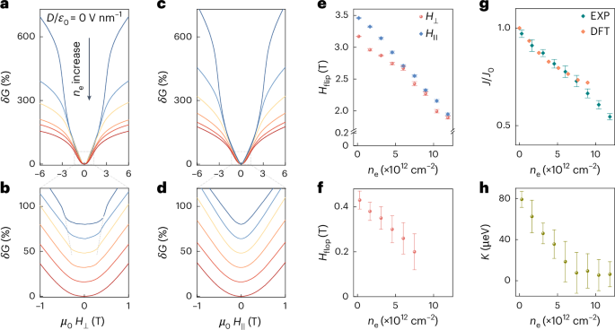
a, Magnetoconductance δG measured at 2 K and zero D/ε0 as a function of out-of-plane magnetic field H⊥, for ne varying from 1.75 × 10¹¹ to 1.2 × 1013 cm−2. The field at which δG starts to flatten corresponds to the spin-flip field (Hflip) and can be precisely determined from the minimum in the second derivative of conductance (G) with respect to H⊥ (c). b, Low-field magnetoconductance measured under H⊥, showing the effect of the spin-flop field (Hflop, indicated by the dash grey line; Hflop is determined by the position of the corresponding peak in d2G/dH2). c, δG measured under the same conditions as in a, with field H∥ applied parallel to the plane. d, Low-field magnetoconductance measured under H∥; as expected, the spin-flop transition is absent. e, Evolution of Hflip (obtained from the minimum in d2G/dH2; Supplementary Fig. 2) for H⊥ and H∥ (red and blue dots, respectively) as a function of ne. Hflip is slightly smaller when the field is applied perpendicular to the plane (e), because of the uniaxial magnetic anisotropy of CrPS4 (Supplementary Note 2). f, Evolution of Hflop for H⊥, as a function of ne. g, ne-dependent interlayer exchange energy ratio J/J0 (cyan diamonds for experimental data, orange diamonds for DFT calculations). J0 is the interlayer exchange energy at the lowest doping, ({J}_{0}^{{rm{DFT}}}) (ne = 0) = 1.1 meV for the DFT calculations, and ({J}_{0}^{{rm{EXP}}}) (ne = 1.75 × 1011 cm−2) = 0.58 meV for the experimental values (a trend towards flattening seen in the DFT calculations at large ne remains to be understood). h, Uniaxial magnetic anisotropy K extracted from Hflip measured for both H⊥ and H∥ (see Supplementary Note 2 for details). The error bars in e and f are estimated from the width of the maximum/minimum in d2G/dH2 used to determine Hflop and Hflip (the width is taken at a 1% deviation from the maximum/minimum; see Supplementary Fig. 3 for an example). The error bars in g and h are calculated by propagating the errors shown in e.
Source data
From these measurements, we extract quantitative values for the parameters determining the magnetic state of the CrPS4 bilayer, the interlayer exchange energy J and the uniaxial magnetic anisotropy K (Methods and Supplementary Note 2). To this end, we express the magnetic energy of the system as E = JM1·M2/Ms2 – K/2 (M1z/Ms)2 – K/2 (M2z/Ms)2 − μ0 H·(M1 + M2), where M1 and M2 are the magnetizations of the two layers owing to the Cr atoms, Ms is the single-layer saturation magnetization (per unit cell) and H is the applied magnetic field. The analysis of the spin-flip transition with in- and out-of-plane field (Fig. 2e) gives the values of J and K shown in Fig. 2g,h, both decreasing upon increasing ne. Surprisingly, the magnetic anisotropy vanishes at ne > 7–8 × 1012 cm−2 (K likely changes sign and the magnetization reorients to be in the plane45, but under these conditions, our magnetoconductance measurements cannot be used to determine its value). The observed trends agree with ab initio calculations (Fig. 2g). The suppression of J can be understood as due to the already established downshift of the conduction band edge in the ferromagnetic state39. Because of this downshift, accumulating electrons increases the energy of the antiferromagnetic state (EAFM) more than that of the ferromagnetic one (EFM) so that the interlayer exchange energy J (related to EFM (ne) – EAFM (ne)) decreases.
We conclude that—when probing the existence of spin-polarized bands in the CrPS4 bilayer—the charge density needs to be limited to values well below 7 × 1012 cm−2, to avoid that the magnetic state of CrPS4 is strongly affected by the accumulated electrons. We also conclude that the influence of the accumulated electrons on the magnetic state is well described by a large change in the values of J and K, and not in the magnetization of the layer where electrons are accumulated. Indeed, as ne is increased up to approximately 1013 cm−2, J changes by a factor of 2 and K vanishes, whereas the change in layer magnetization is smaller than 0.5% (the electron density is only approximately 1% of the density of Cr atoms and the spin of Cr is 3/2). We should therefore analyse the system by considering first that electrons populate states in the conduction band associated with the underlying magnetic structure created by the Cr atoms (determined considering that J and K are functions of ne), and only later consider the effect of the modified layer magnetization.
Hysteretic magneto-transport
In the presence of a perpendicular displacement field and sufficiently low ne, electrons are accumulated in the bottom or top layer depending on the sign of D. They occupy one of the spin-split bands, whose spin polarization is determined by the magnetization of the Cr atoms in the same layer (Fig. 1a). The system has then two possible states (labelled A and B) with opposite spin of the accumulated electrons (Fig. 3a). The two states are energetically degenerate at zero applied perpendicular magnetic field H⊥, and their energies shift in opposite direction when sweeping H⊥ towards positive or negative values, owing to the Zeeman energy of accumulated electrons. Even if the system is initialized in the low-energy state, therefore, it will eventually occupy the high-energy metastable state when the magnetic field is swept and changes sign. More specifically, when the magnetic field is swept from large negative values through the (negative) spin-flop field46, there is no preference between states A and B if D/ε0 = 0. With a finite D, however, the system develops a preference and favours the state with lower energy (as shown in Fig. 3a). As the magnetic field is swept to positive values, the system switches to the other state, resulting in an antiparallel magnetization arrangement, but with the Néel vector reversed (see Extended Data Fig. 3 for details). We then expect the magnetoconductance to be hysteretic if the two states with opposite electron magnetization exhibit different conductance.
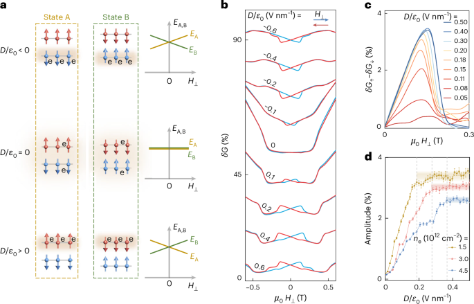
a, At small magnetic field, 2L CrPS4 can be in one of the two states—with opposite magnetization in the top and bottom layers—labelled as A (left column) and B (right column). These states are energetically degenerate (EA = EB) in the absence of gate-induced electrons (ne = 0) or when electrons equally occupy both layers (D/ε0 = 0). The degeneracy is broken at finite ne and perpendicular electric field D/ε0, in the presence of a perpendicular magnetic field. The state with lower energy is determined by the sign of the applied electric and magnetic fields, because the energy difference arises from the Zeeman energy of accumulated electrons that—a low ne—occupy states in one of the two layers (and are therefore spin-polarized with spin pointing in opposite directions; Fig. 1a). b, δG measured at different D/ε0 (legend) at ne = 1.5 × 1012 cm−2. At D/ε0 = 0, no hysteresis is observed owing to the degeneracy of states A and B, as expected. The hysteresis that appears at finite D/ε0 when sweeping H⊥ up or down provides direct experimental evidence for the existence of the two states with different energies in a finite perpendicular magnetic field. c, Magnetoconductance hysteresis, corresponding to the difference between the magnetoconductance measured with field swept up (δG↑) or down (δG↓) for different values of D/ε0 (legend) and constant density ne = 1.5 × 1012 cm−2. The hysteresis amplitude first increases with D/ε0 and then saturates. d, Hysteresis amplitude as a function of D/ε0 for different carrier densities. The saturation threshold of Dsat/ε0 shifts to higher values as the carrier density increases, as indicated by the dashed lines and shaded regions. The error bars in d are estimated from the noise level of the curves in c.
Source data
Figure 3b shows the low-field magnetoconductance measured in a perpendicular magnetic field, at ne = 1.5 × 1012 cm−2, for different values of D/ε0. Hysteresis emerges at finite D/ε0, so that the magnetoconductance differs depending on whether the applied magnetic field is swept from negative to positive (blue curves) or from positive to negative (red curves) values. The hysteresis ends with a sharp jump at approximately μ0 H = 0.2 T, exhibiting a phenomenology typical of easy axis ferromagnets47. No hysteresis is observed for parallel magnetic field, as expected, since in a parallel field states A and B always have the same energy (see Extended Data Fig. 4 for details). The observed behaviour therefore confirms that electrons generate a net magnetization as they populate the spin-split conduction band of the CrPS4 bilayer, owing to the symmetry breaking induced by the applied displacement field (virtually identical behaviour has been seen in another double-gated device; Supplementary Fig. 4). The switching between the two magnetic states may occur with the bilayer staying in a single domain (as in the Stoner–Wohlfarth model47) or by breaking the CrPS4 bilayers into magnetic domains47. In the latter case, reversing the magnetic field sweep direction halfway the hysteresis loop should result in ‘minority’ hysteresis loops, with the magnetoconductance that does not re-trace the curve measured when the magnetic field is swept up to H > Hflop. This is indeed what we observe experimentally (Supplementary Fig. 5).
Figure 3c shows how the magnitude of the magnetoconductance hysteresis evolves upon increasing displacement field D/ε0, with data measured at a fixed carrier density ne = 1.5 × 1012 cm−2. Starting from D/ε0 = 0, δG↑−δG↓ first increases rapidly, before saturating at approximately D/ε0 = 0.18 V nm−1. The dependence of the magnitude (quantified by the peak value of δG↑−δG↓) is summarized by the brown dots in Fig. 3d. Measurements at larger values of accumulated electron density ne exhibit the overall same behaviour (red and blue dots in Fig. 3d), but the displacement field needed to reach saturation increases. The trend is consistent with the behaviour expected for a conduction band spin-splitting induced by the displacement field (as shown in Fig. 1a). As D/ε0 is initially turned on, the spin-splitting is small—much smaller than the Fermi energy corresponding to the accumulated charge density—so that both the spin-up and spin-down bands in the two layers are populated. The population of the two bands is only slightly different, which is why the amplitude of the hysteresis is small. As D/ε0 is increased, the spin-splitting in the conduction band also increases, and so does the difference in population of spin-up and -down bands, which is why the amplitude of δG↑−δG↓ also increases. At sufficiently large D/ε0, the splitting between the spin-up and -down bands becomes larger than the Fermi energy, so that the electrons populate only one of the bands. Past this point, a further increase in D/ε0 does not change the population of the spin-split bands, and δG↑−δG↓ saturates.
This scenario naturally explains why the accumulation of a larger electron density ne requires a larger displacement field to reach saturation. We estimate the value of displacement field at saturation as Dsat/ε0 = ne εr/(e d (m∗/2πℏ2)) by equating the induced electrostatic energy difference between the two layers to the Fermi energy of the electrons occupying one layer (d is the distance between the CrPS4 layers forming the bilayer, εr is the relative dielectric constant (3.9), m* is the effective mass (1.26 times the free electron mass) in CrPS4 (ref. 48), e is the electron charge, and ℏ is Planck’s constant). For ne = 1.5 × 1012 cm−2, Dsat/ε0 ≈ 0.3 V nm−1, close to the experimental value. Both the argument invoked to explain the evolution of the magnetoconductance hysteresis with displacement field and the good correspondence between the estimated and measured values of Dsat/ε0 support the scenario that the conduction band is fully spin-polarized for D/ε0 > Dsat/ε0.
Odd–even effects
To confirm that a vertical displacement field causes a hysteretic magnetoconductance because of the effect of inversion symmetry breaking on the accumulated electrons, we have explored devices realized on 3, 4 and 5 CrPS4 layers (3L, 4L and 5L; Fig. 4). Even (2L and 4L) and odd (3L and 5L) CrPS4 multilayers should exhibit distinctly different behaviour, because in odd layers the magnetization of the top and bottom layers is the same, whereas in even layers it is opposite. Reversing the displacement field polarity, therefore, alters the spin polarization of gate-accumulated electrons only in even layers. In addition, in odd multilayers, the magnetization of the uncompensated layer of Cr atoms (MCr ≠ 0) is nearly thousand times larger than that of the accumulated electrons. Therefore, in odd multilayers, the magnetization is large already in the absence of any accumulated electron and switches at small applied magnetic field (around 0.05 T)37. In other words, in odd layers, the switching between state A and state B (see schematics in Fig. 3 for bilayers) is driven by the uncompensated layer’s magnetization: since the conductance does not depend on whether the Cr magnetization points up or down, the switch between states A and B in odd layers has no measurable effect on transport.
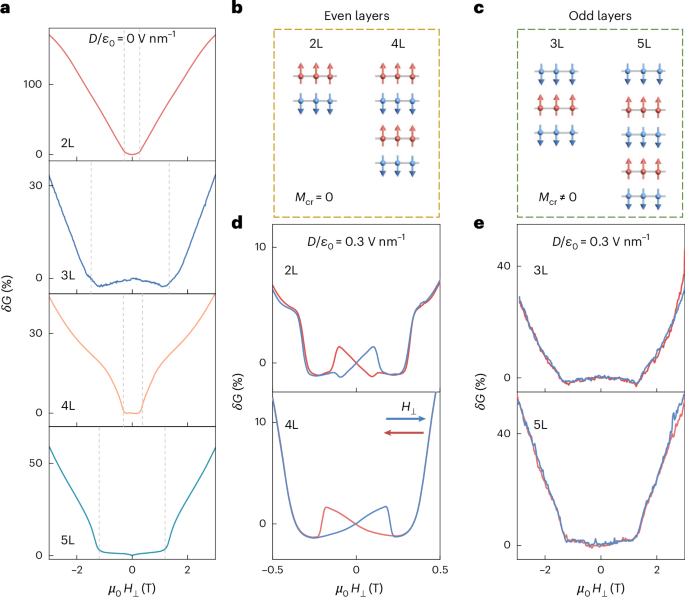
a, Magnetoconductance δG(H) measured at 2 K and zero electric field (D/ε0 = 0, ne ≈ 4.5 × 1012 cm−2) on double-gated devices based on 2L, 3L, 4L and 5L CrPS4 (from top to bottom, see legends). The spin-flop transition (indicated by the dashed lines) in odd layers occurs at 2–3 times larger field than in even layers (approximately 0.5 T), as expected for weakly anisotropic layered antiferromagnets43,49. In the absence of an applied displacement field, no magnetoresistance hysteresis is observed irrespective of layer thickness. b, Schematic representation of the A-type magnetic order in even number of CrS4 layers, where red (blue) arrows represent the magnetization of the Cr atoms in each layer. For even layers, the total magnetization owing to the Cr atoms vanishes. c, Same as in b but for odd number of CrS4 layers. The total magnetization of Cr atoms is finite owing to the presence of an unpaired layer. d, Magnetoconductance δG(H) measured at 2 K on even layers (2L and 4L) at D/ε0 = 0.3 V nm−1 and ne ≈ 4.5 × 1012 cm−2, exhibiting a clear hysteresis when sweeping the perpendicular magnetic field (H⊥). e, Magnetoconductance δG (H, 2 K) measured on odd layers (3L and 5L) at D/ε0 = 0.3 V nm−1 and ne ≈ 4.5 × 1012 cm−2, exhibiting no hysteresis below spin-flop field even when an applied perpendicular displacement field is present.
Source data
Figure 4 shows magnetoconductance data for 3–5L CrPS4. At D/ε0 = 0, no hysteresis is observed below the spin-flop field irrespective of layer thickness, as expected. A very pronounced odd–even effect is evident in the spin-flop transition fields, with even layers transitioning at approximately 0.5 T and odd layers at 2–3 times larger field (Fig. 4a). This difference originates from the magnetization of the uncompensated layer present in odd multilayers (Fig. 4b,c), which shifts the spin-flop transition to higher magnetic field (see earlier work on CrSBr and CrCl3)43,49. More importantly, when an electric field is applied, the behaviour of even and odd layers becomes markedly different. Hysteresis in the magnetoconductance emerges, but only in even layers (Fig. 4d): odd layers continue to show no hysteresis (Fig. 4e). The amplitude of the magnetoconductance hysteresis in 4L CrPS4 is comparable to that of 2L CrPS4, even though detailed aspects are different. For instance, increasing the displacement field from a negative (−0.6 V nm−1) to a positive value (0.6 V nm−1) causes the sign of the magnetoconductance hysteresis in 4L to change multiple times (Supplementary Fig. 6). This is likely because the electronic wavefunctions evolve from being distributed equally over all layers at D/ε0 = 0 to be localized only on the outer layer (top or bottom depending on the sign of D), causing multiple changes in the electronic magnetization. Irrespective of these details, the key conclusion is that the magnetoconductance hysteresis is observed only in even CrPS4 multilayers, owing to inversion symmetry caused by a finite displacement field.
Doping-dependent hysteresis
Finally, we discuss the evolution of the magnetoconductance hysteresis in bilayers as the carrier density is increased past the value at which the uniaxial magnetic anisotropy K vanishes. If the sign of K changes, as we expect for ne > 7–8 × 1012 cm−2, the magnetization in 2L CrPS4 reorients to point in-plane. States A and B then have the same energy at a finite magnetic field, and no switching—hence no magnetoconductance hysteresis—should be observed. This is what we find if we measure the magnetoconductance at a fixed D (D/ε0 = −0.26 V nm−1 in Fig. 5a) for increasing values of ne: the hysteresis becomes less pronounced, the coercive field decreases, and vanishes around ne ≈ 7–8 × 1012 cm−2. Figure 5b,c summarizes the evolution of the hysteretic part of the magnetoconductance (δG↑−δG↓). Figure 5d shows that the coercive field extracted from this data scales with ne as the uniaxial magnetic anisotropy constant (Fig. 2h). Consistently, we also see that the spin-flop transition—proportional to (sqrt{K})—shifts to lower magnetic fields, becomes less pronounced and eventually vanishes (Fig. 5a). Similar trends are observed for 4L CrPS4 (Supplementary Fig. 6).
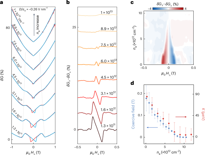
a, Low-field magnetoconductance δG(H⊥) measured for increasing values of accumulated electron density ne (legend), at constant D/ε0 = −0.26 V nm−1 (see Supplementary Fig. 7 for analogous data at positive D/ε0). The hysteresis caused by the finite magnetization of electrons occupying spin-polarized bands becomes less pronounced—and the magnetic field at which the hysteresis ends (that is, the coercive field) becomes smaller—upon increasing ne. Both quantities eventually vanish at approximately 7–8 × 1012 cm−2. The feature associated to the spin-flop transition (indicated by the grey dashed lines) also shifts to lower magnetic fields, becomes less pronounced and eventually disappears on the same ne scale. b,c, Amplitude of the magnetoconductance hysteresis (δG↑−δG↓) obtained from a for different values of ne (b) and colour plot of ({delta G}_{uparrow })−({delta G}_{downarrow }) as a function of ne and H⊥ (c), both showing that the hysteresis vanishes at ne ≈ 7−8 × 1012 cm−2. d, The carrier density evolution of the coercive field extracted from b and c, and of the uniaxial magnetic anisotropy K extracted from the analysis of the spin-flip field in parallel and perpendicular magnetic field, shows that the two quantities are proportional. The error bars for the coercive field correspond to the width of the jump shown in b. K and its error bars are extracted using the same method used to extract the data shown in Fig. 2e.
Source data
Conclusion
The switchable magneto-transport hysteresis reported here shows directly the relation between spatial symmetry breaking—inversion symmetry in the present case—and the existence of spin-polarized bands in antiferromagnets. Controlling spatial symmetries using FETs based on 2D antiferromagnetic semiconductors introduces new functionalities, possibly relevant for antiferromagnetic spintronics, such as the ability to switch on and off spin-dependent transport at will, in principle at high frequency. Furthermore, double-gated CrPS4 bilayers provide a very promising platform to realize gate-induced conductors with near unity spin polarization50, that is, transistors in which not only the flow of charge but also the flow of spin is controlled. The evolution of the amplitude of hysteretic magnetoconductance with displacement field (Fig. 3d) strongly suggests that at a sufficiently large D and low electron density, only one spin-polarized band is occupied, implying that in double-gate CrPS4 bilayer transistors, the dominant spin of the electrons responsible for charge transport can be controllably switched by gate. Conceiving feasible experiments to validate this conclusion—that is, to directly measure the spin polarization of the accumulated electrons as a function of displacement field—is a key milestone for upcoming work.
Finally, when the mobility of charge carriers will be improved, we expect double-gated transistors of CrPS4 bilayers to give control over the sign of anomalous Hall effect. At zero perpendicular electric displacement field—in the absence of spin polarization—no anomalous Hall effect should be observed. As the displacement field is turned on, the anomalous Hall effect should emerge with a sign determined by the sign of D, which fixes the sign of the spin polarization. Gate switchable spin polarization and anomalous Hall effect have never been investigated earlier in bilayer antiferromagnets, and we expect that improving the material quality may allow exploring these phenomena and discovering others.
Methods
Device fabrication
The h-BN/CrPS4/graphite (Gr)/h-BN heterostructures were assembled using a dry pick-up and transfer technique with PDMS-PC stamps in an N2-filled glove box (H2O <0.1 ppm, O2 <0.1 ppm). CrPS4 multilayers were obtained via micromechanical exfoliation inside the glove box from bulk crystals purchased from HQ Graphene. The chemical composition and stoichiometry of CrPS4 bulk crystals were verified using energy-dispersive X-ray spectroscopy in a scanning electron microscope, with elemental mapping showing a uniform distribution and an atomic ratio of Cr:P:S as 16.92:16.60:66.48, consistent with the expected 1:1:4 stoichiometry38. Graphene and h-BN flakes were prepared by mechanical exfoliation onto SiO2/Si substrates. The CrPS4 crystals were encapsulated with top and bottom h-BN layers. Separate graphite stripes acted as source–drain electrodes and were connected to metallic pads via edge contacts located far from the CrPS4 crystal. The edge contacts and metallic pads were fabricated using electron-beam lithography, reactive-ion etching, electron-beam evaporation of 10 nm Cr followed by 50 nm Au, and a lift-off process. Cr/Au contact electrodes were also deposited on the top h-BN to form the top gate. As the bottom gate electrode, we used the highly doped Si substrate, with the SiO2 layer serving as gate dielectric together with the bottom h-BN crystal. In total, we fabricated nine devices using thin CrPS4 layers. We fabricated one device each for 2L, 3L and 4L in a single-gate configuration, with only the bilayer and four-layer devices exhibiting hysteresis. To study the independent effects of the electric field and doping, we fabricated two 2L devices, two 4L devices, one 3L device and one 5L device in a double-gate configuration. The thickness of CrPS4 was determined using optical contrast and Raman spectroscopy (see Extended Data Fig. 2 for details).
Transport measurement
Low-noise homemade electronics in combination with commercial electronics was used to bias the top and bottom gate electrodes, to apply source–drain voltage and to measure the current. Top-gate voltage (VTG) and bottom-gate voltage (VBG) were swept to adjust the doping density (ne = [Ct (VTG − VTGTH) + Cb (VBG − VBGTH)]/e) and the electric displacement field (D/ε0 = [(VTG − VTGTH)/dt − (VBG − VBGTH)/db]/2). Ct and Cb are top- and bottom-gate capacitance per unit area; VTGTH and VBGTH are threshold voltages when sweeping the back gate and top gate, respectively; dt is the thickness of the top h-BN; db is the combined thickness of bottom h-BN and SiO2 layers. Low-temperature transport measurements were conducted in an Oxford Instruments cryostat equipped with a superconducting magnet and a 3He insert.
Antiferromagnetic two-site model
To model the energetics of the bilayer, we assume that the ferromagnetic intralayer exchange coupling is so strong (compared with the weak antiferromagnetic interlayer exchange coupling and the external magnetic field) that each layer can be considered as a single unit with uniform magnetization. Each layer thus behaves as a macroscopic spin that is coupled antiferromagnetically to its neighbour, so that the average magnetic energy per unit cell can be written as43
where J is the antiferromagnetic interlayer exchange coupling, K is the magnetic anisotropy energy favouring out-of-plane orientation, M1 and M2 are the magnetization vectors of the two layers and H is the applied magnetic field. Here Ms = 2gμBS is the saturation magnetization (per unit cell) for a single layer, which can be easily computed from the nominal valence state of Cr atoms in CrPS4 (corresponding to S = 3/2).
Density functional theory calculations
The total energy of the bilayer in the ferromagnetic and antiferromagnetic configurations has been computed from first principles using density functional theory (DFT) as implemented in Quantum ESPRESSO distribution51,52. Atomic positions for the bilayer have been extracted from the bulk relaxed crystal structure38. We have verified that, relaxing the atomic positions, the interlayer distance in the bilayer is only marginally changed with respect to the bulk material. The total energy is obtained adopting the Perdew–Burke–Ernzerhof exchange-correlation functional53 with pseudopotentials taken from the Standard Solid-State Pseudopotential (SSSP) accuracy library (v1.0)54 (cut-offs of ~40 Ry and ~320 Ry for wavefunctions and density). Hubbard corrections have not been included in the calculations. The interlayer exchange energy (per unit cell) is then evaluated as half the energy difference between the ferromagnetic and antiferromagnetic configurations, J = (EFM − EAFM)/2. The 2D nature of the system is taken into account by using a Coulomb cut-off while the effect of doping is simulated using a double-gate field-effect set-up55. To sample the small Fermi surface at finite doping, a dense 24 × 24 × 1 Monkhorst–Pack grid over the Brillouin zone is adopted, with a Gaussian smearing of 6.4 meV.
Responses