The enhanced ferroelectric properties of flexible Hf0.85Ce0.15O2 thin films based on in situ stress regulation

Introduction
Since Böscke et al. first observed ferroelectricity in Si-doped HfO2 materials in 20111, research has found that HfO2-based ferroelectric thin films possess outstanding advantages, such as environmental friendliness, good thermal stability, compatibility with CMOS processes, and the ability to maintain excellent ferroelectricity at the nanoscale2,3,4,5. Ferroelectric memory devices based on HfO2 thin films, with their unique advantages, provide new possibilities for overcoming the limitations in CMOS compatibility and microscale integration in traditional ferroelectric memories1,6,7, thereby becoming the focus of research for the next generation of ferroelectric memory devices.
The preparation of ferroelectric thin films with excellent performance is crucial for the development of ferroelectric memory technology. There are studies indicating that the ferroelectricity of HfO2-based thin films is attributed to the orthorhombic phase with space group Pca211,8 and Pmn219,10, and the rhombohedral phase R3m11,12,13. Despite the controversy surrounding the existence of multiple phase states, current research on the regulation of ferroelectricity in HfO2-based thin films is primarily focused on the orthorhombic Pca21 phase. The mechanism of ferroelectric polarization switching in HfO2-based thin films is attributed to the movement of tricoordinate oxygen atoms along the c-axis within the Pca21 phase, resulting in changes in the polarization state14,15,16. However, this phase, existing between the tetragonal phase (t-phase) and the monoclinic phase (m-phase), is a metastable phase that cannot remain stable under free conditions. Researchers have utilized methods similar to those employed in the study of other ferroelectric thin-film materials to regulate the ferroelectric metastable phase of HfO2-based thin films. Several commonly studied factors include element doping17,18,19,20,21, thin film thickness22,23,24, and stress modulation25,26,27,28,29. Among these factors, stress modulation significantly influences the ferroelectric polarization of thin films. Park et al. have shown that when the thickness of the thin film is reduced to a certain extent (resulting in excessive internal stress), its hysteresis loop exhibits antiferroelectric properties25. This implies that as the internal stress gradually increases, the thin film undergoes a transition process from a non-ferroelectric monoclinic phase to a ferroelectric stable orthorhombic phase, and finally to a non-ferroelectric tetragonal phase. Experimental studies conducted by Shiraishi et al. have demonstrated that the ferroelectricity of Hf0.5Zr0.5O2 thin films is strongly influenced by in-plane stress, which primarily originates from thermal stress resulting from differences in thermal expansion coefficients between the substrate and the thin film30. Experimentally, the influence of stress on the ferroelectric properties of HfO2-based thin films may be attributed to the stress-induced alteration in the proportion of the ferroelectric o-phase during the rapid thermal annealing process31,32,33,34,35. Although numerous scholars have made progress in studying the influence of stress on HfO2-based ferroelectric thin films, the field currently lacks systematic and comprehensive research methods. There are few studies that provide detailed comparisons and analyses of the effects of different stress conditions on the ferroelectric properties of thin films while maintaining other experimental parameters constant. Additionally, research on determining the appropriate stress to achieve a high proportion of the ferroelectric steady-state phase is still inadequate. The traditional method of utilizing diverse substrates to induce stress brings about various interface effects that may interfere with the ferroelectric performance, and this is a problem that needs to be addressed.
Addressing the aforementioned issues, this study proposes a novel stress modulation strategy for HfO2-based ferroelectric thin films. During the high-temperature annealing process, different in situ stresses are applied to the thin films, and this approach allows the thin films to undergo crystalline growth while maintaining a bent state. We systematically investigate the influence of different in situ stress forms and magnitudes on the ferroelectric properties of flexible Ce-doped HfO2 thin films and successfully determine the optimal conditions for stress modulation. Utilizing X-ray diffraction (XRD) and SEM characterization techniques, we reveal the effects of in situ stress annealing on the thin film structure. Additionally, we utilize piezoelectric force microscope (PFM) technology to explore the domain-switching behavior and domain wall migration characteristics of the films. Finally, by testing the optimally modulated flexible Ce-doped HfO2 ferroelectric thin films under conditions of bending stress and high temperatures, we validate the effectiveness and stability of our control method.
Result and discussion
Brief preparation process and characterization of light transmittance for thin films
Figure 1 illustrates the brief preparation process of the flexible Ce-doped HfO2 ferroelectric thin films annealed under different stress bending conditions. The thin films are annealed in three bending states of 12.5, 10, and 7.5 mm, respectively, and the conventional annealed thin film is represented as “unbent”. In this study, the annealing of thin films under stress is defined as follows: the state in which the thin film surface is convex is denoted as “+” indicating tensile stress applied to the thin film, while the state in which the thin film surface is concave is denoted as “−” indicating compressive stress applied to the thin film. According to Supplementary Eq. (1) in the Supporting information, the strains corresponding to the aforementioned radius of curvature are approximately ±0.2%, ±0.25%, and ±0.33%, respectively. This method can adjust the grain size of the thin film by affecting the growth kinetics of the thin film, thereby regulating the thin film’s performance. The transmittance of the flexible Ce-doped HfO2 ferroelectric thin films annealed at unbent, +10 and −10 mm is measured using a UV–visible spectrophotometer in the visible light wavelength range (380–780 nm). Within the visible light spectrum, the transmittance of all thin films still reaches 80%, indicating that the thin films prepared in this study possess high transparency in the visible range.

The preparation process and control mechanism of flexible Ce-doped HfO2 ferroelectric thin films annealed by in situ stress loading.
Electrical performance testing of thin films
The basic electrical performance test results of the flexible Ce-doped HfO2 thin films annealed under in situ stress are shown in Fig. 2. Figure 2a depicts the P–E hysteresis loops of the flexible cerium-doped HfO2 ferroelectric thin films grown under the “+” bending annealing states, under the influence of a smaller electric field of 2.2 MV/cm. As the bending annealing radius decreases, the Pr value of the thin films exhibits a trend of initially increasing and then decreasing, with the performance enhancement being more significant in the +10 mm annealed thin film. The inset in Fig. 2a depicts the saturated hysteresis loop of the +10 mm annealed thin films, with the 2Pr = ~24.7 μC/cm2, and 2Ec = ~2.02 MV/cm. The extracted 2Pr value of the thin films is compared visually, as shown in Fig. 2b. The 2Pr value of the unbent annealed thin film is 9.7 μC/cm2, and the 2Pr value of the +10 mm annealed thin film is 18.2 μC/cm2. Compared with the unbent annealed thin film, the +10 mm annealed thin film exhibits better rectangularity in the hysteresis loop, and its ferroelectric properties are significantly enhanced, with a 2Pr enhancement of ~87.6%. Data on 2Pr and 2Ec values for other thin films are presented in Table 1. The 2Pr value of the thin film annealed at +7.5 mm also increases, but the hysteresis loop indicates that an antiferroelectric transition underwent under the influence of an electric field. To further investigate the effect of an external electric field on the 2Pr value, Fig. 2c presents the curves of these values as a function of the external electric field. Additionally, these curves are normalized for intuitive comparison of the 2Pr variation, as shown in Supplementary Fig. 1a. As the electric field gradually increases, the polarization switching in the +10 mm annealed thin film occurs the fastest. It can be observed that when the external electric field is 2.8 MV/cm, all thin films reach saturation. The hysteresis loops of the thin films are shown in Supplementary Fig. 1b, along with related data in Supplementary Fig. 1c. At this point, the unbent annealed thin film has a 2Pr value of 23.1 μC/cm2 and a 2Ec value of 2.32 MV/cm, and the 2Pr of the +10 mm annealed thin film (24.7 μC/cm2, higher than the unbent annealed film) and 2Ec (2.02 MV/cm, about 13% lower than the unbent annealed film) are both superior to the unbent annealed thin film. Figure 2d depicts the P–E hysteresis loops of the thin films grown under the “−” bending states under the influence of a smaller electric field of 2.2 MV/cm. As the bending annealing radius decreases, the Pr value of the thin films also exhibits a trend of initially increasing and then decreasing, with the ferroelectric performance reaching optimization when annealed at −10 mm, and it exhibits a good hysteresis loop shape. The inset in Fig. 2d illustrates the saturated hysteresis loop of the −10 mm annealed thin films. The 2Pr of the −10 mm annealed thin film is ~24.5 μC/cm2, while the 2Ec is ~2.04 MV/cm. By comparing the 2Pr values of the thin films, as shown in Fig. 2e and Table 2, the 2Pr value of the −10 mm annealed thin film is 16.6 μC/cm2, which is ~71.1% higher than that of the unbent annealed thin film. Figure 2f displays the curves of the 2Pr value varying with the external electric field, and the curves are normalized as shown in Supplementary Fig. 1d. It is also observed that the thin film annealed at −10 mm exhibits the fastest polarization switching speed. When the external electric field reaches saturation (Supplementary Fig. 1e and f), the 2Pr value (24.5 μC/cm2, higher than the unbent annealed thin film) and 2Ec value (2.04 MV/cm, about 12% lower than the unbent annealed thin film) of the −10 mm annealed thin film are both superior to the unbent annealed thin film. According to the results mentioned above, the ferroelectric properties of the thin films are optimized when the annealing radius is 10 mm, whether annealed under in situ tensile or compressive stresses. Thin films fabricated under this bending annealing condition can more easily achieve polarization switching, thereby exhibiting better ferroelectric properties. This suggests that applying certain tensile and compressive stresses to the thin films during the annealing crystallization stage can effectively reduce the polarization switching barrier.
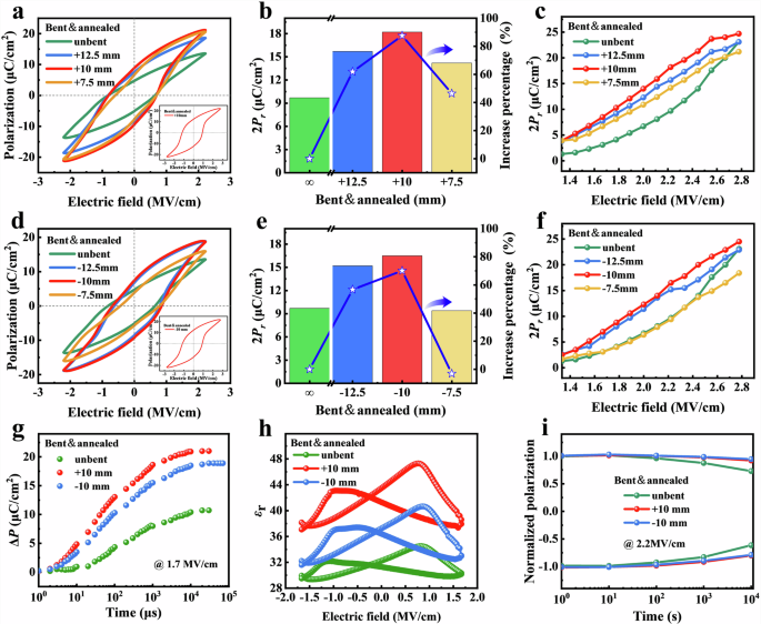
a The P–E hysteresis loops of the thin films annealed by in situ tensile stress, and the inset figure shows the saturated hysteresis loop of the +10 mm annealed thin films. b Comparison chart of the 2Pr values of thin films annealed by in situ tensile stress. c The curves of 2Pr of thin films annealed under in situ tensile stress as a function of the applied electric field. d The P–E hysteresis loops of the thin film annealed by in situ compressive stress and the inset figure shows the saturated hysteresis loop of the −10 mm annealed thin films. e Comparison chart of the 2Pr values of thin films annealed by in situ compressive stress. f The curves of 2Pr of thin films annealed under in situ compressive stress as a function of the applied electric field. g The polarization switching characteristic curves. h εr–E hysteresis loops. i Retention performance.
Based on the pulse sequence (Supplementary Fig. 2a), the speed of domain switching in the thin film is evaluated by detecting the amount of polarization switching under different pulse widths at a fixed write pulse amplitude, and the test samples are selected as unbent, +10, and −10 mm annealed thin films. The ferroelectric polarization of the thin films annealed at +10 and −10 mm can switch rapidly after short pulse application, and the degree of their switching is significantly higher than that of the unbent thin film. When the switching reaches saturation, the polarization switching amount ΔP of the film annealed at +10 mm bending (~21 μC/cm2) and that of the film annealed at −10 mm bending (~19 μC/cm2) are both significantly higher than that of the unbent film (~11 μC/cm2). It can be seen that the films annealed at +10 and −10 mm bending radii can quickly change their polarization direction under the action of an electric field and achieve a larger polarization intensity. Supplementary Fig. 2b illustrates the normalized curve (ΔP/2Ps) for the three thin films, where Ps represents the saturation polarization. It can be observed that the switching speeds of +10 and −10 mm annealed thin films are noticeably faster than that of the unbent thin film. At the same time, we find that the relative permittivity (εr) of +10 and −10 mm annealed thin films is greatly increased, as shown in Fig. 2h. Ferroelectric thin films with high relative permittivity exhibit significant polarization response and charge storage capacity. These thin films are capable of rapidly generating polarization response and maintaining a stable polarized state under the influence of an external electric field, and this ability is crucial for the polarization switching process of the thin films under frequent electric field cycles. Therefore, ferroelectric materials with high relative permittivity typically demonstrate improved reliability. The retention performance within the time range of 1–104 s is also tested and the curves are normalized, as shown in Fig. 2i. After 104 s, the polarization attenuation of the unbent annealed thin film is ~32.8%. However, the polarization attenuation rates of the thin films annealed at +10 mm (~13.9%) and −10 mm (~13.3%) are significantly lower than that of the unbent annealed thin film. The +10 and −10 mm annealed thin films exhibit superior retention performance.
Structural characterization of thin films
Figure 3a shows the XRD patterns of the flexible Ce-doped HfO2 ferroelectric thin films annealed under in situ tensile stress. An obvious characteristic diffraction peak is observed at 2θ ≈ 30.5° for each thin film, which corresponds to (111)o/(101)t. The relative intensity of the ferroelectric o-phase diffraction peak noticeably increases when the bending annealing radius is +10 mm, indicating a potentially higher content of the ferroelectric o-phase. The bending annealing radius varies from +12.5 to +10 mm, and a characteristic peak corresponding to (002)o/(110)t appears near 35°, which almost disappears as the bending radius continues to decrease to +7.5 mm. This observation potentially further reveals a trend, whereby as the bending annealing radius decreases, the content of the ferroelectric o-phase in the film initially increases and then decreases. Figure 3b displays the XRD patterns of the flexible Ce-doped HfO2 ferroelectric thin films annealed under in situ compressive stress. The XRD patterns of the −12.5 and −10 mm annealed thin films both exhibit characteristic diffraction peaks corresponding to (111)o/(101)t at 2θ ≈ 30.5°. Among them, the relative intensity of this peak in the thin film annealed at −10 mm bending is enhanced compared with the unbent thin film. Additionally, characteristic peaks corresponding to (002)o/(110)t are also observed near 35° for the thin films annealed at −12.5 and −10 mm bending. However, for the thin film annealed at −7.5 mm bending, the relative intensities of these characteristic diffraction peaks are not significant, indicating a weaker diffraction effect. Due to the presence of a mixed diffraction peak for the o/t phases near 30.5°, we perform peak deconvolution on this diffraction peak to better observe the variation in the ratio of o/t-phases. The specific results are presented in Supplementary Fig. 3. This result suggests that the tensile and compressive stresses applied during the annealing crystallization stage have a significant impact on the crystal structure of the flexible Ce-doped HfO2 ferroelectric thin films. In conjunction with the electrical properties of the thin films annealed under different in situ stresses, as shown in Fig. 2, we speculate that within a certain stress, range may facilitate the formation of the ferroelectric o-phase, whereas excessive stress could potentially lead to the unstable existence of the ferroelectric phase.
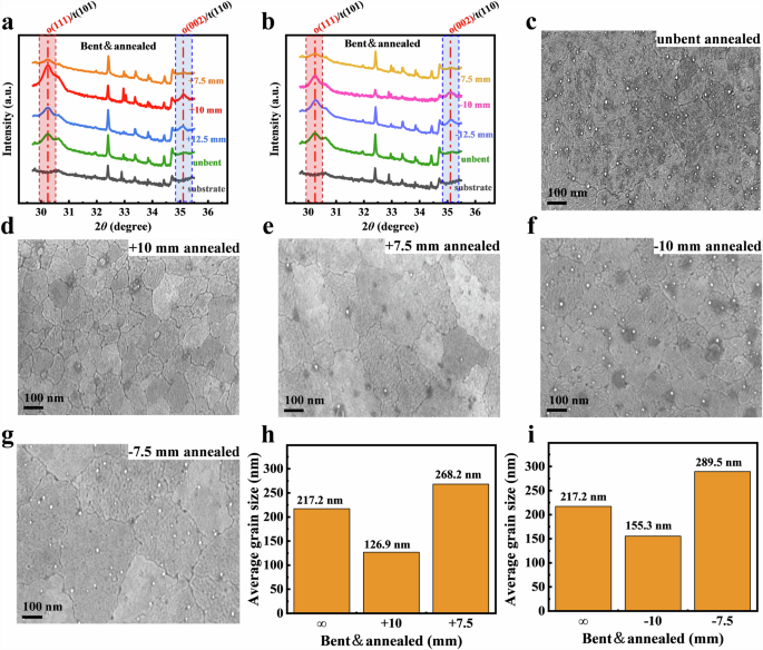
a The thin films annealed in “+” bending state. b The thin films annealed in “−” bending state. SEM characterization. c Unbent, d +10 mm, e +7.5 mm, f −10 mm, g −7.5 mm annealed thin films. h The average grain size of thin films annealed in “+” bending state, i the average grain size of thin films annealed in “−” bending state.
The surface morphology of the thin films is analyzed using scanning electron microscopy (SEM) to further investigate the influence of different bending and annealing radii on the grain characteristics of the flexible Ce-doped HfO2 ferroelectric thin films. This analysis supplements the microstructural characterization that XRD analysis cannot provide. The characterized samples are selected as unbent annealed, +10 and −10 mm annealed thin films with the best performance modulation, and +7.5 and −7.5 mm annealed thin films with deteriorated performance, as shown in Fig. 3c–g. From the figures, clear grain boundaries and continuously distributed grains are observable, indicating that the samples we prepared all have good crystallinity. Among them, the grains of the unbent annealed thin film appears in large sheet-like sizes (Fig. 3c). In contrast, the grain size of the +10 mm annealed thin film significantly decreases (Fig. 3d), exhibiting a denser crystalline structure. Meanwhile, the grain size of the +7.5 mm annealed thin film is found to be larger (Fig. 3e). The grain size of the −10 mm annealed thin film decreases (Fig. 3f), while the grain size of the −7.5 mm annealed thin film increases (Fig. 3g). The grain size distribution of each thin film sample is statistically analyzed based on the SEM images, as shown in the Supplementary Fig. 4. It can be observed that the unbent thin film mostly consists of large-sized grains, with grain sizes primarily distributed in the range of 200–250 nm. For the +10 mm annealed thin film, the grain sizes are more concentrated between 100 and 120 nm, with a rare occurrence of large-sized grains. In contrast, the thin film annealed at +7.5 mm bending exhibits a relatively high frequency of grain sizes falling within the 250–300 nm range. The grain sizes of the thin films annealed at −10 and −7.5 mm bending are mainly concentrated in the ranges of 140–160 and 250–300 nm, respectively. Further fitting analysis reveals that the grain size distributions of all thin film samples exhibit Gaussian characteristics. Specifically, for the unbent, +10, and +7.5 mm annealed films, their standard deviations (ω) in grain size distribution are 133.1, 50.6, and 129.8, respectively. For the −10 and −7.5 mm annealed thin films, the standard deviations (ω) are 120.8 and 96.3, respectively. Compared with the unbent annealed thin film, both the +10 and −10 mm annealed thin films exhibit better uniformity in grain size distribution. The average grain sizes of the thin film samples are shown in Fig. 3h and i. The average grain sizes of the unbent, +10, and +7.5 mm annealed thin films are 217.2, 126.9, and 268.2 nm, respectively. Additionally, the average grain sizes of the −10 and −7.5 mm annealed thin films are 155.3 and 289.5 nm, respectively. This discovery demonstrates that the in situ stress annealing method employed by us can effectively regulate the grain size of the thin film, successfully achieving grain refinement. Especially for the +10 mm thin film annealed under in situ tensile stress, its grain size is small and uniform. The experimental results demonstrate that our regulation method can significantly influence the grain size of the thin films. The application of appropriate stress disrupts the arrangement of atoms or ions within the crystals, thereby increasing the probability of new nuclei formation, leading to a reduction in grain size. However, when the applied stress is excessively high, the thin films may undergo cracking, resulting in an increase in grain size. The grain size effect of hafnium oxide-based ferroelectric thin films plays a crucial role in optimizing the thin film’s performance. Smaller grain sizes lead to the dominance of surface energy, the lower energy of the ferroelectric phase. Therefore, it is more favorable for the existence of ferroelectric phase grains, allowing for a greater number of reversible ferroelectric domains and stronger switching capability36,37. This is also the reason why the ferroelectric properties of the thin film annealed at +10 and −10 mm are superior to the unbent thin film, as discussed earlier (Fig. 2).
Characterization of domain switching performance in thin films
The polarization switching in ferroelectric thin films involves multiple consecutive stages, including domain nucleation, longitudinal growth, lateral growth, and domain merging. This process is influenced by various factors, including the thickness of the thin film, its crystal structure, and fabrication conditions. By optimizing these factors, one can enhance the efficiency of domain switching, thus achieving better control over the final polarization state of the thin film. In order to specifically evaluate the effective enhancement of ferroelectricity and ferroelectric polarization switching ability in the +10 and −10 mm annealed thin films, we have employed PFM technology to investigate the behavior of domain switching under the influence of electric field. Figure 4a–c shows the out-of-plane phase images of the overall domain switching for the unbent, +10 and −10 mm annealed thin films, a clear boundary can be observed with distinct color contrast on the left and right sides, indicating different directions of domain switching in this region. It is noteworthy that the +10 and −10 mm annealed thin films, optimized through in situ stress annealing, demonstrate significantly enhanced uniformity in domain switching compared with the unbent thin film. Further contrast analysis reveals that the domain switching in +10 and −10 mm annealed thin films is more comprehensive. Additionally, the average phase angles of domain switching are approximately 140°, 170°, and 150° for the unbent, +10, and −10 mm annealed thin films, respectively. The phase difference of the domain switching theoretically should be 180° for fully switchable domains in ferroelectric thin films. However, the actual phase difference of the domain switching in the thin films did not reach this theoretical value, possibly due to the pinning effect of non-ferroelectric phases and defects within the thin film, as well as the testing conditions being under a small electric field rather than a saturating electric field. The local single-point PFM amplitude and phase hysteresis loops are also characterized as shown in Supplementary Fig. 5, and it can be found that the thin films annealed at +10 and −10 mm exhibit better domain switching behavior.
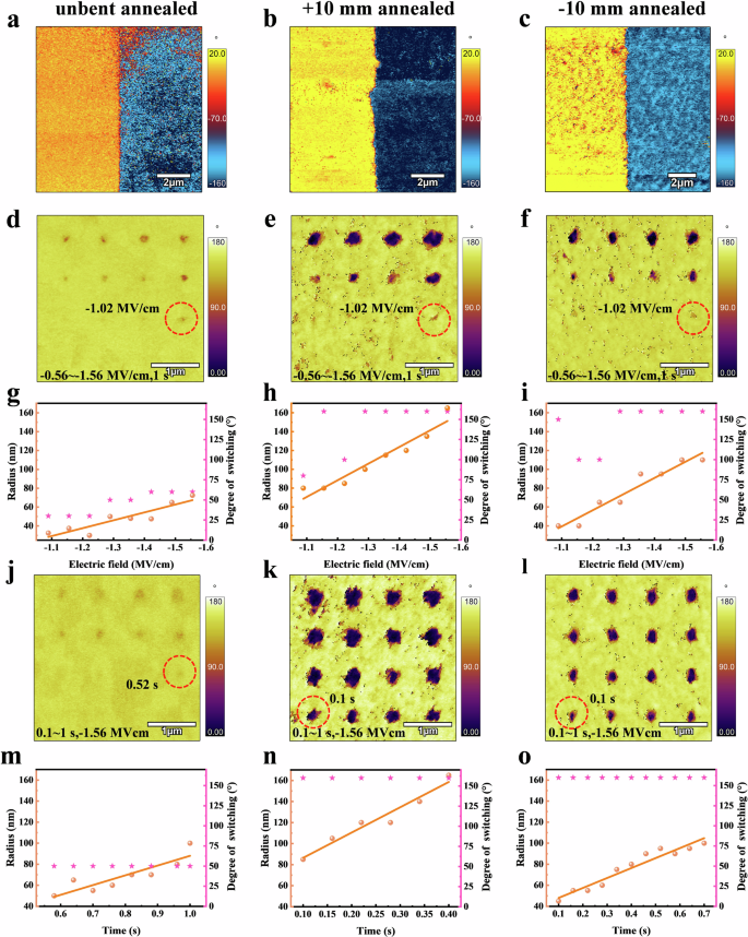
a Unbent, b +10 mm, and c −10 mm annealed thin films. Fixed time is 1 s, which is influenced by the gradient pulse electric field. d–f Out-of-plane phase map of upward-polarized domain arrays. d Unbent, e +10 mm, and f −10 mm annealed thin films. Statistical analysis of the domain switching radius and degree of domain switching in the upward-polarized domains. g Unbent, h +10 mm, and i −10 mm annealed thin films. The fixed electric field is −1.56 MV/cm, subject to the influence of gradient pulse width. j–l Out-of-plane phase map of upward-polarized domain arrays. j Unbent; k +10 mm and l −10 mm annealed thin films. m–o Statistical analysis of the domain switching radius and degree of domain switching in the upward-polarized domains. m Unbent; n +10 mm and o −10 mm annealed thin films.
The effect of the pulse electric field on the domain wall migration of thin films is studied by using PFM to observe the domain switching behavior and explore the difference of domain nucleation threshold electric field. Firstly, an electric field of 1.56 MV/cm is applied to the 3.5 μm × 3.5 μm region of the thin film to polarize it in a downward direction. Then, a gradient pulse electric field ranging from −0.56 to −1.56 MV/cm is applied, and the duration of the electric field application is 1 s. Finally, the domain structure within this region is examined, and a 4 × 4 array of upwardly polarized domains is obtained. Figure 4d–f shows the out-of-plane phase maps of the domain polarized up-switching region for the unbent, +10, and −10 mm annealed thin films. The differences in the degree of domain switching among the three thin films can be observed through the color contrast within the figures. Specifically, the threshold electric field for upward polarized domain nucleation in the unbent, +10, and −10 mm annealed thin films is about −1.02 MV/cm. After reaching the nucleation threshold electric field, the domain switching in the unbent annealed thin film is not obvious (Fig. 4d). In contrast, upon the application of pulse electric fields, the out-of-plane phase maps for the thin films annealed at +10 and −10 mm exhibit noticeable color changes. When the applied external electric field reaches the nucleation threshold electric field of −1.02 MV/cm, the domain radius of the +10 and −10 mm annealed thin films significantly increases with the increase of the electric field (Fig. 4e and f). The domain switching degree and radius of three types of thin films are statistically analyzed, and the relationship between domain radius and gradient pulse electric field is linearly fitted, as shown in Fig. 4g–i. The corresponding domain wall mobility can be obtained by calculating the slope of the fitting curve, as shown in Table 3. The phase difference during domain switching of the unbent thin film measures ~60°, and the radius of the domain radius after switching is very small, ~72.5 nm (Fig. 4g). This is due to the large grain size of the unbent thin film, and relatively low content of the as-grown ferroelectric stable phase. Consequently, under conditions of a small electric field, the switching behavior of the thin film is not particularly pronounced. Within the range of the applied gradient pulse electric field, the domain wall mobility of the unbent thin film measures ~83.6 nm/(MV/cm). The +10 mm annealed thin film exhibits the largest domain radius of about 165 nm and a switching phase difference of about 160° (Fig. 4h). Within the range of the applied gradient pulse electric field, the domain wall mobility of this thin film is ~176.8 nm/(MV/cm), demonstrating a significant advantage of high mobility. As for the −10 mm annealed thin film (Fig. 4i), its maximum domain switching radius is ~110 nm, accompanied by a switching phase difference of nearly 160° and a domain wall mobility of ~171.4 nm/(MV/cm). During the domain switching process with the same orientation, while the three types of thin films exhibit the same domain nucleation threshold electric field, the thin films annealed under in situ stress (bending annealing radii of +10 and −10 mm) undergo more complete domain switching and faster domain wall mobility. Furthermore, there exists a correlation between the domain wall mobility and the applied pulse electric field, where a faster domain wall movement corresponds to a more rapid increase in domain radius as the external pulse electric field increases.
By employing gradient pulse width to investigate the differences in domain switching nucleation time among three samples. Furthermore, with the domain switched state at the maximum action time of 1 s designated as the near-saturation state, we investigate the practical electric field application time required for the thin film to reach the near-saturation state of domain switching, as well as the domain migration rate at this state. This approach facilitates a deeper understanding of the domain wall migration behavior in thin films under various pulse width conditions. First, applying an electric field of 1.56 MV/cm to the 3.5 μm × 3.5 μm region of thin films makes the polarization direction downward. Then, a gradient pulse width of 0.1–1 s (with a fixed electric field of −1.56 MV/cm) is applied to the region, and the out-of-plane phase diagram of the 4 × 4 array with domain polarization upward is obtained, as shown in Fig. 4j–l. The nucleation threshold time for upward polarized domains in the unbent annealed thin film is found to be 0.52 s (Fig. 4j). In the out-of-plane phase diagram, only faint traces of domain switching are observed as the pulse width increases, indicating the difficulty of its domain switching behavior to occur. In contrast, upon the application of an electric field, domain switching occurs immediately in both the +10 and −10 mm annealed thin films (Fig. 4k and l). The nucleation threshold time for the upward-polarized domains is <0.1 s and the switching is nearly complete. The nucleation threshold time for upward-polarized domains in the +10 and −10 mm annealed thin films is ~80.8% lower than that in the unbent annealed thin film. A statistical analysis is conducted on the radius and degree of domain polarization upward switching in three types of thin films. Additionally, a linear fitting is performed to investigate the relationship between the switching domain radius and the applied gradient pulse width, as illustrated in Fig. 4m–o. The corresponding domain wall migration rates are obtained through the slopes of the fitted curves, as summarized in Table 4. As the time gradually approaches 1 s, the domain switching in the unbent thin film reaches a near-saturation state. At this point, the phase difference for domain switching in the unbent thin film is ~50°, the radius of the switching domain is ~100 nm, and the domain wall migration rate, obtained through statistical analysis, is ~92.8 nm/s (Fig. 4m). For the +10 mm annealed thin film, as the pulse width increases, the switching radius shows a trend of lateral expansion. As the time approaches 0.4 s, the domain switching of the thin film nears saturation. At this point, the domain wall migration rate of the +10 mm annealed thin film is ~240.5 nm/s, with a domain switching phase difference of about 160° and a switching domain radius of ~165 nm (Fig. 4n). For the −10 mm annealed thin film, at 0.7 s, the domain switching reaches a near-saturation state with a radius and switching phase difference of approximately 100 nm and 160°, respectively (Fig. 4o). At this stage, the domain wall migration rate of the −10 mm annealed film is ~94.7 nm/s. The results indicate that specific stress annealing conditions (with bending annealing radii of +10 and −10 mm) have a significant positive impact on the domain evolution behavior of flexible Ce-doped HfO2 ferroelectric thin films, facilitating rapid domain switching in the thin films. The influence of gradient pulse electric field and gradient pulse width on the migration characteristics of downward-polarized ferroelectric domain walls in the three thin films is shown in Supplementary Fig. 6. It is also found that the polarization down-domain switching ability of the +10 and −10 mm annealed thin films is superior to that of the unbent annealed thin film.
The above implies that the growth of the thin film under a bent state (with a bending annealing radius of +10 and −10 mm) significantly enhances the ferroelectric domain switching capability. The macroscopic ferroelectric performance of the film is mainly determined by the domain structure and switching ability of ferroelectric grains within the thin film. Consistent with the previous characterization of ferroelectric performance (Fig. 2), the +10 and −10 mm annealed thin films exhibit better ferroelectric domain switching performance compared with the unbent annealed thin film, with the optimum improvement observed in the +10 mm annealed thin film.
Reliability testing of thin films
In order to assess the stability and reliability of the thin film with optimal regulation, we applied bending stress and high-temperature testing conditions to the +10 and −10 mm annealed thin films. Mechanical bending tests are conducted on the +10 and −10 mm annealed thin films using metal molds with different bending radii (as shown in Supplementary Fig. 7) to study the changes in their electrical properties. In the tests, a positive sign (+) indicates that the thin film is under tensile stress, while a negative sign (−) indicates that the thin film is under compressive stress. Specifically, this study involves applying bending stress to the +10 and −10 mm annealed thin films that have already been fabricated to test their performance stability and reliability. The objective is to observe changes in their performance under different bending stress conditions, which differ from the stress applied during the fabrication process. Under the same applied electric field conditions (as shown in Fig. 5a, b, e, f), the hysteresis loops measured in different stress-inflicted bending states of the films almost perfectly overlap with the hysteresis loops measured in the flat state. This indicates that the thin films prepared by annealing under the 10 mm bent state can maintain excellent ferroelectric performance under various external stress loads. This suggests that the preparation method of annealing while maintaining a bent state can effectively control the performance of the thin film and achieve stable optimization, unaffected by variations in external applied stress. From Fig. 5c and g, it can be observed that the retention performance of the +10 and −10 mm annealed thin films is not compromised when restored to the originally grown bent state, and the thin films still exhibit excellent characteristics. The ferroelectric properties of the two thin films are tested over a temperature range from room temperature (25 °C) to high temperature (150 °C), as shown in Fig. 5d and h. With the gradual increase in temperature from 25 to 75 °C, the hysteresis loops of the thin film remain relatively stable, showing no significant changes. However, as the temperature continues to rise to 125 °C and further to 150 °C, a slight increase in the Pr value of the hysteresis loop is observed. This change may be attributed to the intensification of lattice thermal motion under high-temperature conditions. Overall, the Ce-doped HfO2 ferroelectric thin films annealed at +10 and −10 mm exhibit excellent high-temperature resistance. Even at a high temperature of 150 °C, their ferroelectric properties remain stable. The experimental results demonstrate that the +10 and −10 mm annealed thin films exhibit excellent stability and reliability, which not only fully validates that our regulation method is a stable and effective optimization approach for thin films, but also provides strong support for the idea that flexible HfO2-based ferroelectric thin films have great potential applications in the field of flexible electronics38.
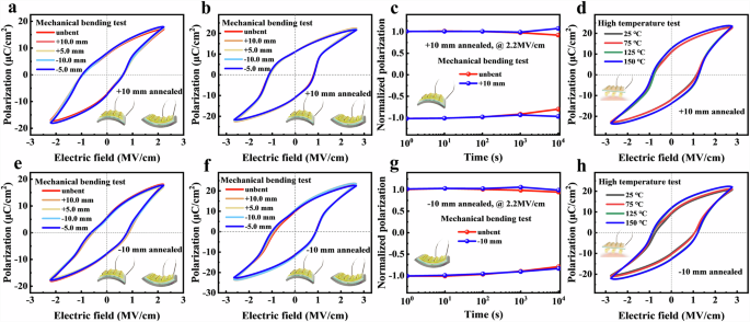
The P–E hysteresis loops of +10 mm annealed thin film under external bending stress: a under 2.2 MV/cm electric field, b under saturated electric field, and c retention performance curves. d The P–E hysteresis loops of +10 mm annealed thin film at high temperature. The P–E hysteresis loops of −10 mm annealed film under external stress: e under 2.2 MV/cm electric field; f under saturated electric field; and g retention performance curves. h the P–E hysteresis loops of −10 mm annealed thin film at high temperature.
In summary, the in situ stress annealing method utilized in our study effectively modulated the performance of flexible HfO2-based ferroelectric thin films, which show notable performance differences among films annealed under different bending radii. Notably, the thin films demonstrated optimal performance modulation when annealed at bending radii of +10 and −10 mm. Under this bending annealing radius, the thin films have a reduced grain size and an increased content of the ferroelectric orthorhombic o-phase, leading to a higher number of ferroelectric domains switching. Therefore, the thin films exhibit improved ferroelectric properties and domain-switching performance. Under relatively low electric fields, compared with the unbent thin film, the 2Pr value of the +10 mm thin film annealed under in situ tensile stress increases by 87.6%, while the 2Pr value of the −10 mm thin film annealed under in situ compressive stress increases by 71.1%. Additionally, the domain switching ability of +10 and −10 mm annealed thin films is effectively enhanced. Furthermore, the +10 and −10 mm annealed thin films maintained good ferroelectric properties under applied stress and high-temperature conditions, indicating that the optimized film obtained through our control method exhibits stable performance that remains unaffected by external conditions. In this study, we experimentally obtained the stress regulation range for the metastable-to-stable phase transition and enhanced the domain switching capability, providing guidance for the preparation of flexible HfO2-based ferroelectric thin films with high performance and a high proportion of stable phase. This is beneficial for certain applications, such as electronic devices, where the polarization state of the thin film can be controlled and manipulated using lower electric fields. It enhances the performance and reliability of thin films, enabling the realization of devices with lower power consumption and higher performance.
Methods
Preparation of the bottom electrode
An ITO bottom electrode was deposited on a fluorophlogopite mica substrate [KMg3(AlSi3O10)F2] (Hefei Kejing Material Technology Co., Ltd., Hefei, China) using a magnetron sputtering film deposition system. Initially, the fluorophlogopite mica was attached to the sample holder of the magnetron sputterer using conductive double-sided adhesive tape. Then, the sample holder was covered with a shield and automatically transported into the deposition chamber. Once the pressure inside the deposition chamber was adjusted to below 8 × 10⁻² mbar, a high-purity ITO ceramic target was selected. The sputtering parameters included a power setting of 60 W. After a preliminary sputtering of 10 s the glow was checked through the observation window to ensure it was normal; following confirmation, the sputtering duration was extended to 600 s. Argon gas was introduced, and the pressure was maintained stable via an automatic control system. After sputtering was completed, the mica piece with the ITO electrode layer was removed, sealed, and stored for later use.
Preparation of the precursor
In this study, cerium (Ce) was chosen as the doping element for the HfO2-based ferroelectric thin film (Hf0.85Ce0.15O2). First, the required amount of hafnium acetylacetonate (C20H28HfO8, 97%, Toshima Manufacturing Co., Ltd.) was weighed on a balance with weighing paper, mixed with glacial acetic acid in a beaker, and stirred for 20 min on a magnetic stirrer. Subsequently, the required amount of cerium nitrate hexahydrate (Ce(NO3)3·6H2O, 99.95%, Shanghai Aladdin Biochemical Technology Co. China) and acetylacetone (C5H8O2, AR, Tianjin Kemiou Chemical Reagent Co., Ltd. Tianjin, China) were sequentially added into the beaker and stirred until homogeneous to obtain a precursor solution with a concentration of 0.1 mol/L.
Fabrication of the thin film
In this study, the substrate materials, the preparation of precursor solution and the spin-coating process, drying and pyrolysis process parameters of the thin films deposited refer to our previous research work38, and the specific experimental procedures are provided in the supplementary materials (shown in Supplementary Fig. 8). The precursor solution was deposited on the ITO bottom electrode using a spin-coating method. The spin coater parameters were set to 500 rpm for 15 s at low speed and 3000 rpm for 30 s at high speed. After spin coating, a wet film was obtained. The wet film was subjected to drying (180 °C, maintained for 180 s) and pyrolysis (350 °C, maintained for 180 s) in a rapid thermal annealing furnace.
After repeating the spin-coating, drying, and pyrolysis processes multiple times, a dry gel thin film is obtained. The thin film is then placed in metal molds with different bending radii and transferred to a rapid thermal annealing furnace for annealing at 800 °C under a nitrogen atmosphere for 400 s. After the annealing process is completed, the thin film is removed from the metal mold and flattened, with a thickness of ~90 nm. Finally, following mask treatment, the direct current sputtering method is used to grow an Au electrode with a radius of 100 μm, forming the MFM capacitor structure.
Characterization methods
This study employs the Ultima IV XRD instrument of the Japan Science Council and the Sigma 500 thermal field emission scanning electron microscope manufactured by ZEISS of Germany to characterize the microstructural information of the flexible Ce-doped HfO2 ferroelectric thin films annealed under different stress conditions. The P–E characteristics, retention, and polarization switching characteristics of the thin films are characterized using the TF Analyzer 3000 system. The dielectric properties of the thin films are tested using the semiconductor device parameter testing and analysis system, Agilent B1500A, developed and produced by Agilent Technologies in the United States. The polarization switching characteristics of the thin films ferroelectric domains are investigated using the Litho-PFM and SS-PFM methods of the Asylum Research MFP-3D Infinity atomic force microscope produced by Oxford Instruments.


Responses