Topological phase transition in quasi-one-dimensional bismuth iodide Bi4I4

Introduction
Topological quantum phase transitions (TQPTs) represent a fascinating type of phase transitions characterized by global topological invariants, which diverge from the conventional symmetry-breaking phase transitions described by local order parameters. TQPTs not only hold significant scientific implications for elucidating topological properties under external perturbations1,2,3,4,5 but also pave an avenue for the utilization of topological quantum materials with high tunability in future electronic and spintronic devices6,7,8,9. Throughout a TQPT, the ground-state wavefunction evolves with a controlling parameter such as strain, chemical substitution, electric field, and temperature10,11,12,13,14,15,16,17, typically associated with a change in the energy gap of the boundary states.
Recently, quasi-one-dimensional (quasi-1D) bismuth halides Bi4X4 (X = Br, I) have garnered great research attention owing to the abundant topological quantum phases in this family compounds, including strong/weak topological insulator18,19,20, higher-order topological insulator21,22,23, and Weyl semimetal24. These intriguing topological quantum phases are sensitive to the stacking sequence and interlayer coupling of Bi4X4 layers constituting the bulk crystals25,26,27. By manipulating external conditions, e.g., tuning temperature, applying strain or chemical substitution, TQPT can be established and feasibly controlled.
Taking Bi4I4 as an example, monolayer Bi4I4 consists of arrays of chains along the b axis, which has been verified as near a 2D quantum spin Hall (QSH) insulator/normal insulator phase boundary28,29,30. Bulk α/β-Bi4I4 share the same chain structure except that the α-phase comprises two Bi4I4 chains relatively shifting along the a axis in a unit cell (Fig. 1a, b). Consequently, the interaction between the QSH edge states in each Bi4I4 monolayer is distinctive in the two phases. For β-Bi4I4, the monolayers stack along c with the metallicity of the side surface preserved by the symmetry, realizing a WTI phase4,12,31,32,33,34. By contrast, the adjacent QSH edge states are in different chemical environments in α-Bi4I4. Therefore, the hybridization between adjacent QSH edge states induces gapped (100) surface states (Fig. 1b, c). Remarkably, for particular stacking sequences, gapless modes, namely topological hinge states, survive at the hinges of the crystal as enforced by the higher-order bulk-boundary correspondence (see the red dots in Fig. 1b)27,35. Since the dimensional difference between the bulk and conducting boundary mode is larger than 1, this intriguing topological state is classified as a HOTI. Upon increasing temperature, α-Bi4I4 undergoes a structural transition to β-Bi4I436, establishing a temperature-induced TQPT.

a The crystal structure of α-Bi4I4. The black lines indicate the unit cell. b Schematic illustration of the boundary states on the (100) surfaces. Each dot represents the QSH edge state of a Bi4I4 monolayer. The yellow-dot pair in an ellipse and red dots represent the quantum-hybridized (100) surface states and the topological hinge states, respectively. c Illustration of the electronic structure of α-Bi4I4 on the (100) side surface. The gray, yellow, and red curves indicate the bulk, surface, and hinge states, respectively. d–f The same as (a–c) except for β-Bi4I4. The green dots in (e) and green curves in (f) represent the topological surface states on the (100) surface of β-Bi4I4. g Cross-section image of the (010) surface of α-Bi4I4 with atomic resolution measured with scanning transmission electron microscope (STEM). h X-ray diffraction measurements of α-Bi4I4. The STEM and XRD measurements are performed at 298 K.
Angle-resolved photoemission spectroscopy (ARPES), serving as a powerful tool to elucidate the electronic structure of single crystals, has been performed to unravel the band structure of bismuth halides26,37,38,39,40. While high-resolution laser-ARPES experiments have shown evidence for the HOTI phase in α-Bi4Br4, the investigation of Bi4I4 is more intricate35,41,42. Gapless (100) surface states have been observed in β-Bi4I435,41, confirming its non-trivial topological property. However, there are still debates on the existence of gapless surface states on the (001) surface, making it elusive whether β-Bi4I4 is a WTI or strong topological insulator (STI). As for α-Bi4I4, although a gapped (100) surface state has been detected at the ({bar{Gamma }}_{100}) point35 in accordance with the theoretical prediction, further confirmation is still required to ascertain whether the side surface states are fully gapped over the whole surface Brillouin zone (especially at the (bar{Z}) point) and conclusively identify the HOTI phase. Moreover, only a subtle change of the width of ARPES spectra was observed across the structural transition35, with the temperature-evolution of the fine electronic structure, especially the surface gap, yet to be investigated.
In this work, by performing laser-based micro-ARPES measurements with high energy and momentum resolution37,43, we systematically investigate the temperature evolution of the electronic structure of Bi4I4. At low temperatures, we observe gaps of about 40 meV and 5 meV at the ({bar{Gamma }}_{100}) and (bar{Z}) points on the (100) surface, confirming the HOTI phase of α-Bi4I4 (Fig. 2c). With increasing temperature, we directly observe the evolution of the gapped surface states into a gapless Dirac fermion across the transition temperature TS~300 K. The magnitude of the gap shows a thermal hysteretic behavior, confirming the first-order nature of the TQPT. Moreover, our measurements unveil that a fully gapped (001) surface of β-Bi4I4, which, together with the gapless topological surface states (TSSs) on the (100) surface, compellingly evidences the WTI phase of β-Bi4I4 (Fig. 2d). Our experimental observations are in excellent agreement with ab-initio calculations and provide more systematic insights into the TQPT of quasi-1D Bi4I4.
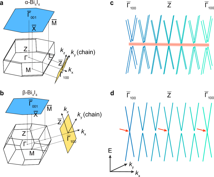
a, b Bulk and surface Brillouin zones of α/β-Bi4I4 with high-symmetry points indicated, respectively. c, d Schematics showing the surface band structure of HOTI phase of α-Bi4I4 and WTI phase of β-Bi4I4. The blue curves and the red line indicate the (100) surface states and in-gap hinge states, respectively. The red arrows indicate the location of the gapless Dirac fermions.
Results
Electronic structure and topological property of α-Bi4I4
Figure 3a shows the ARPES spectrum of α-Bi4I4 at the ({bar{Gamma }}_{100}) point on the (100) surface. We resolve valence and conduction bands of the (100) surface states, characterizing the splitting feature and surface gap caused by hybridization of the QSH edge states from adjacent Bi4I4 layers (Fig. 1c). According to the curvature spectra in Fig. 3c, the energy gap between the valence and conduction band is estimated to be about 31 meV (the peak-to-peak gap between the band crossing points at ({bar{Gamma }}_{100}) is about 40 meV). At the (bar{Z}) point, the surface states exhibit a Dirac-cone-like dispersion with a gap of about 7 meV (Fig. 3b, d). Our measurements agree with the calculation in Fig. 3e, f. The gapped dispersion at (bar{Z}) can be further evidenced by fitting the Dirac dispersion as shown in Fig. 3b. The band dispersion is firstly extracted by fitting the momentum distribution curves (MDCs) to the Lorentzians (represented by the green dots). Then the upper and lower branches of the extracted dispersion are fitted to linear dispersions. The energy interval between the crossing points of the upper and lower branches indicates an energy gap of about 5 meV at the Dirac point, in line with the curvature analysis (Fig. 3d) and the theoretical calculation (Fig. 3f).
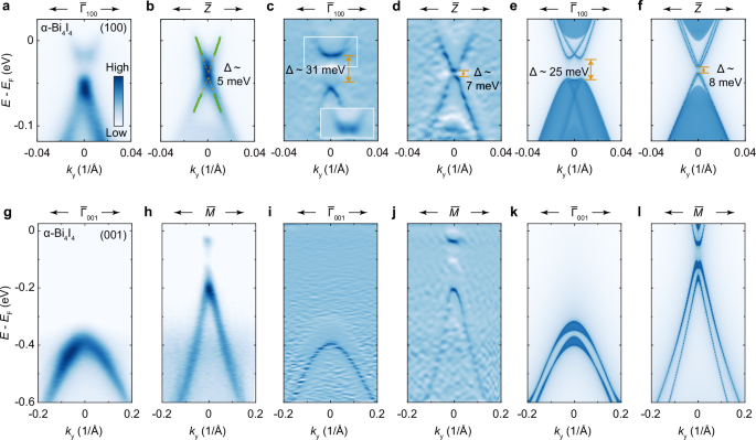
a, b Band structure of the (100) surface states at the ({bar{Gamma }}_{100}) and (bar{Z}) points measured by laser-based micro-ARPES. The green dots in (b) are determined by fitting the momentum distribution curves (MDCs) to Lorentzians and the yellow dashed lines are the fit of the extracted dispersion to the massive Dirac-fermion dispersion. c, d Curvature plots of the ARPES spectra in (a) and (b). e, f (100) surface-projected band structures calculated at the ({bar{Gamma }}_{100}) and (bar{Z}) points, respectively. g, h ARPES spectra of α-Bi4I4 at the ({bar{Gamma }}_{001}) and (bar{M}) points on the (001) surface. i, j Curvature plots of the ARPES spectra in (g) and (h). (k, l) (001) surface-projected band structures calculated at the ({bar{Gamma }}_{001}) and (bar{M}) point, respectively. Data were measured along the chain direction at 80 K using LH-polarized 7-eV laser.
Figure 3g, h shows the laser-ARPES spectra of α-Bi4I4 measured on the (001) surface with their curvature plots shown in Figs. 3i and 3j, respectively. Around the ({bar{Gamma }}_{001}) point, we observe a band gap over 395 meV without the conduction band observed. At the (bar{M}) point, we observe a direct band gap of about 170 meV. Both the experiments at ({bar{Gamma }}_{001}) and (bar{M}) are well reproduced by the theoretical calculation of the bulk states, suggesting the absence of topological surface states on the (001) surface of α-Bi4I4. Therefore, our results on the (001) and (100) surfaces confirm the HOTI phase of α-Bi4I4, resembling the results of α-Bi4Br437. We do not resolve explicit signals from the topological hinge states, possibly due to the weak photoemission intensity from the hinge states and relatively small (100) surface gap of α-Bi4I4.
Electronic structure and topological property of β-Bi4I4
Next, we examine the electronic structure of the (100) surface of β-Bi4I4 at 316 K. As shown in Fig. 4a, b, β-Bi4I4 shows a gapless Dirac fermion dispersion at both ({bar{Gamma }}_{100}) and (bar{Z}) point. As to (001) surface, β-Bi4I4 exhibits a band gap of 330 meV (between the valence band top and EF) and 125 meV (between the valence band top and the conduction band bottom) at the ({bar{Gamma }}_{001}) and (bar{M}) points, respectively, similar to α-Bi4I4 (Fig. 4c, d). Compared to α-Bi4I4, the valence and conduction band of β-Bi4I4 shift up slightly with a weak residual spectral weight of the conduction band at EF. We do not observe any signature of topological surface states on the (001) surface, which is in line with the WTI phase of β-Bi4I4.
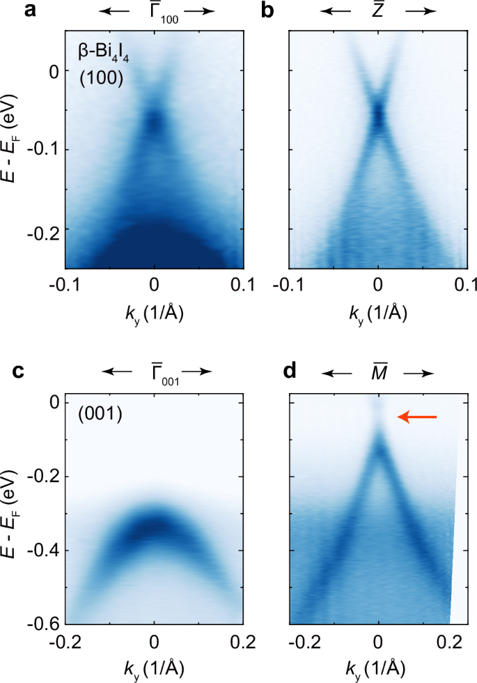
a, b ARPES spectra of β-Bi4I4 at ({bar{Gamma }}_{100}) and (bar{Z}) point on the (100) surface, respectively. c, d ARPES spectra of β-Bi4I4 at ({bar{Gamma }}_{001}) and (bar{M}) point on the (001) surface, respectively. The red arrow indicates the energy gap at the (bar{M}) point. The spectra were measured along the chain direction at 316 K using LH-polarized 7-eV laser.
Topological phase transition of Bi4I4
In order to study the topological phase transition of bismuth iodide, we perform systematic ARPES measurements at different temperatures across TS. At 80 K, the data at the ({bar{Gamma }}_{100}) point (Fig. 5a) clearly shows a gap, consistent with the (100) surface states of α-Bi4I4 in Fig. 3a. With increasing temperature up to around 310 K, the energy interval between the surface valence and conduction band at the ({bar{Gamma }}_{100}) point slightly decreases. The spectra also get blurred at high temperatures, which may indicate a preclude of crystal transformation related to the structural transition instead of thermal broadening effect35. Prominently, above TS, the surface gap is suddenly suppressed and the dispersion shows a single gapless Dirac dispersion (Fig. 5g), which confirms the WTI phase of β-Bi4I4 together with the gapped spectra on the (001) surface (Fig. 4). Simultaneously, the spectrum becomes much sharper with the full width at the half maximum changed from about 0.01 ({{text{AA }}}^{-1}) (302 K) to 0.007 ({{text{AA }}}^{-1}) (316 K). This band sharpening of surface states is because of the bilayer splitting of α-Bi4I4 (Fig. 1c) and has been revealed by the previous experiments35. As the temperature decreases, the spectrum recovers at low temperatures and the surface gap reemerges (Fig. 5h–k).
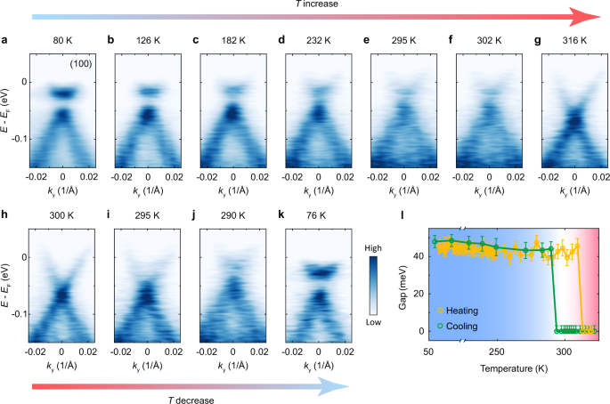
a–k ARPES spectra of the (100) surface states at the ({bar{Gamma }}_{100}) point of α-Bi4I4 (a–g) and (bar{Z}) point of β-Bi4I4 (h–k). The thick arrows indicate the heating or cooling process. Please note the ({bar{Gamma }}_{100}) point of α-Bi4I4 and the (bar{Z}) point of β-Bi4I4 correspond to almost the same photoelectron emission angle. l Temperature evolution of the (100) surface gap showing a hysteresis loop.
The temperature evolution of the (100) surface gap extracted by double-Lorentzian fitting the EDC at ({bar{Gamma }}_{100}) is summarized in Fig. 5l, which exhibits a thermal hysteresis loop near the structural transition. Specifically, an α-phase characterization is maintained up to about 310 K in the heating process, which can be confirmed by features such as surface gap and band sharpness mentioned above (Fig. 5a–f). While in the cooling process, a β-phase spectrum with a sharp single Dirac cone is evident even at 295 K in Fig. 5i, in significant contrast to Fig. 5e detected at the same temperature. The hysteresis in the (100) surface gap indicates that Bi4I4 undergoes a first-order structural phase transition accompanied by the topological phase transition from a HOTI to a WTI, in accordance with our ab-initio calculation.
Discussion
For a long time, 2D QSH insulators, hosting symmetry-protected 1D edge states immune to backscattering, are expected to promote the development of dissipationless electronics and spintronics devices4,5,44. However, the complicated fabrication of 2D-material devices limits the exploration and application of the 1D edge states. By contrast, 1D topological quantum materials such as Bi4X4 can be relatively easily synthesized and naturally harbor highly directional topological boundary states with spin-momentum locking property, which are beneficial for the preservation of coherent quantum states. The quasi-1D nature of Bi4X4 further allows for the integration into nanowire configurations that are natural and ideal for device engineering. In particular, the novel HOTI phase with hinge states is promising for dissipationless transport, efficient charge-to-spin conversion, topological quantum computation based on the Majorana zero modes, and the realization of spin-triplet superconductivity45,46,47,48,49,50,51,52,53. Furthermore, the TQPT between HOTI and WTI phases in Bi4I4 bridged by a first-order structural transition provides a unique opportunity for the controllable manipulation of the topological boundary states near room temperature.
To conclude, we systematically investigate the electronic structure and its temperature evolution of Bi4I4. We observe a fully gapped (100) surface state of α-Bi4I4, supporting the identification of its HOTI phase. Our measurements at high temperatures confirm the WTI phase of β-Bi4I4 by detecting its gapped (001) band structure and gapless (100) TSS. More importantly, we detect the thermal hysteresis loop of the gap in the (100) surface states. Our study unravels the fine band structure of Bi4I4 with unprecedented precision and provides solid evidence on the TQPT between HOTI and WTI phases bridged by the structural transition. Our results provide deeper scientific insight and pave the way to promising applications on the novel topological quantum properties of quasi-1D Bi4I4.
Methods
Single crystal synthesis and characterization
High-quality Bi4I4 single crystals were synthesized using a solid-state reaction and chemical vapor transport method54. Figure 1g presents the cross-section image by atomic-resolved scanning transmission electron microscope, which confirms the crystal structure and the high quality of our samples.
Laser-based μ-ARPES measurements
Laser-based μ–ARPES measurements with a sub-micron spatial resolution were conducted at Tsinghua University with the 7-eV laser generated by a KBe2BO3F2 (KBBF) crystal and focused by an optics lens43. The samples were cleaved in-situ under UHV better than 1 × 10⁻¹⁰ mbar and the data were collected by Scienta DA30L electron analyzer. The total energy and angular resolutions were set to 3 meV and 0.2°, respectively.
Ab-initio calculations
First-principles calculations were conducted to investigate the electronic properties and topological band characteristics of bulk Bi4I4 using the Vienna ab-initio simulation package55. The Heyd-Scuseria-Ernzerhof hybrid functional (HSE06) was employed to describe the exchange-correlation potential56. Experimental lattice parameters were used, with the energy cutoff for the plane-wave basis set to 300 eV. Maximally localized Wannier functions (MLWFs) for the p-orbitals of Bi and I atoms were constructed using the WANNIER90 code on a 6 × 6 × 3 k-point mesh57. These MLWFs were subsequently applied to build ab initio tight-binding models. Surface electronic structures were calculated by combining the ab-initio tight-binding models with the surface Green function method using our in-house code58.


Responses