Towards sustainable perovskite light-emitting diodes
Main
The advent of light-emitting diodes (LEDs) has reshaped how humans utilize light. LEDs emit light through electroluminescence, offering energy-efficient lighting and revolutionizing display technologies. Among the various emerging LED technologies, perovskite LEDs (PeLEDs) have gained increasing attention owing to their advantages, such as a lightweight design, flexibility and a wide colour gamut. PeLEDs can be fabricated using low-energy techniques and earth-abundant materials. They have achieved high efficiencies across the three primary colours: red, green and blue (RGB)1,2,3. Furthermore, the stability of PeLEDs has markedly improved in recent years2,4, demonstrating promising potential for commercialization5.
Environmental, economic and technical factors are critical for the commercialization of innovative technologies and for evaluating their sustainable potential6. To comprehensively assess these factors, a life-cycle perspective is essential7. While numerous studies have evaluated the life-cycle impacts of emerging perovskite solar cells8,9,10,11, their findings cannot be directly extrapolated to PeLEDs due to the fundamental difference in energy conversion mechanisms: solar cells convert light into electricity, whereas LEDs convert electricity into light. Moreover, the operation of PeLEDs across multiple wavelengths necessitates diverse functional layer materials, requiring different analyses for devices of varying colours. To identify effective pathways towards the sustainable commercialization of PeLEDs, a comprehensive life-cycle assessment (LCA) encompassing all stages is necessary.
Here we examine emerging PeLED technology from a life-cycle perspective, focusing on commercialization-oriented sustainability, including environmental, economic and technical performance. Specifically, we analyse the environmental impact and economic cost of PeLEDs on the basis of a detailed life-cycle inventory (LCI) assessment of 18 state-of-the-art PeLEDs, spanning RGB, white and near-infrared (NIR) wavelengths. We identify technical pathways for sustainability improvement by focusing on key factors across the entire life cycle. Furthermore, we propose relative impact mitigation time (RIMT) as a new parameter to quantify the lifetime required for PeLEDs to achieve sustainability from a life-cycle perspective. As a comprehensive life-cycle study on PeLEDs, this work provides data and methodologies to illuminate the sustainable potential of PeLEDs and guide future research on analogous technologies.
LCAs of lab-scale PeLEDs
We commence our LCA with lab-scale PeLED devices to derive insights relevant to the industrial development of PeLEDs. A comprehensive life cycle encompasses all stages, from cradle to grave. For PeLEDs, these stages include raw material acquisition, manufacturing, distribution, use and end of life. Environmental impacts across these stages arise from the exchange of substances and electricity. Despite the varying material compositions of PeLEDs reported in the literature, they share essential functional layers, as illustrated by a uniform system boundary in Fig. 1. We selected 18 state-of-the-art technologies from the literature for analysis, covering RGB, white and NIR colours. Supplementary Tables 1–5 provide their technical details and naming conventions. From these, we compile detailed LCIs that encompass the production and emissions associated with PeLEDs (Supplementary Appendix A). Definitions of system boundaries and the application of inventories are detailed in Methods.
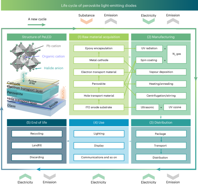
A typical PeLED device comprises a glass substrate, ITO anode, hole transport layer, perovskite emissive layer, electron transport layer and metal cathode. The active area is the region covered by all functional layers. The perovskite layer typically consists of organic or metal cations, Pb cations and halide anions. The cradle-to-grave life cycle of a PeLED covers five stages: (1) raw material acquisition, (2) manufacturing, (3) distribution, (4) use and (5) end of life. Substances and electricity are the primary forms of exchange throughout the life cycle. UV, ultraviolet.
The LCA results reveal that the environmental impacts of PeLEDs stem primarily from the inputs of substances and electricity during production. Eight significant impact categories, selected from the 18 ReCiPe 2016 categories12, are depicted in Fig. 2. Overall, PeLEDs—excluding three NIR devices, which are addressed separately—exhibit comparable environmental impact profiles. This similarity arises from their identical device structures, where variations in substance and electricity consumption for electron/hole transport and perovskite layers are insufficient to cause substantial differences. The primary contributors to these impacts are raw materials, particularly organic cleaning solvents (for example, acetone and isopropanol). The remaining impacts arise predominantly from device assembly, where electricity consumption accounts for more than 99%, with nitrogen gas (N2) gloveboxes and vapour deposition being the most energy-intensive sources. The distribution stage (that is, transport) contributes less than 5% of the total impacts, and its optimization depends on industrial resources rather than PeLED design. The use stage, where environmental impacts exhibit a dynamic relationship with usage time, is excluded from this section and will be discussed subsequently. At the end-of-life stage, landfill disposal is employed for lab-scale devices. Although this approach contributes minimally to total impacts, recycling is recommended for future industrial applications to reduce raw material input. Numerically, the principal environmental impacts of a 1 m2 lab-scale PeLED over its life cycle include human carcinogenic toxicity at 1.81–2.13 kg 1,4-dichlorobenzene- (1,4-DCB-) equivalent, freshwater ecotoxicity at 1.64–2.20 kg 1,4-DCB-equivalent, fossil resource scarcity at 52.72–55.15 kg oil-equivalent, marine ecotoxicity at 2.16–2.85 kg 1,4-DCB-equivalent and freshwater eutrophication at 0.03–0.04 kg phosphorus- (P-) equivalent. Supplementary Tables 8–15 and Supplementary Figs. 7–12 provide further numerical results and descriptions of abbreviations.
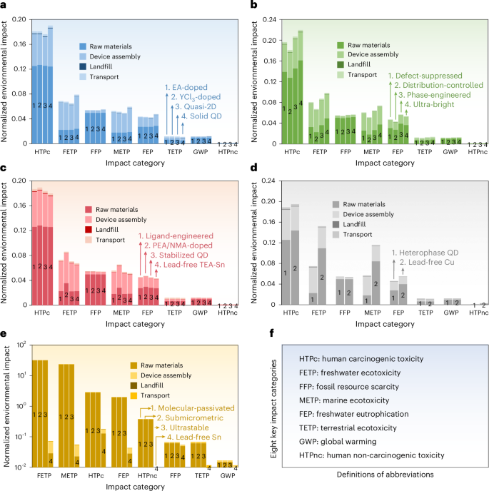
a–e, Eight key environmental impact categories for 18 different PeLEDs (prepared using different approaches) with colours blue (a), green (b), red (c), white (d) and NIR (e). Contributions of different life-cycle stages are shown, assuming identical operating conditions. Impacts from the use stage, dependent on usage time, are excluded and will be discussed subsequently. For numerical comparability, the environmental impacts of each category are normalized using the 2010 global emissions and resource extraction inventory47. NIR device values are presented on a logarithmic scale. f, Definitions of abbreviations for the eight key impact categories. EA, ethylammomium; 2D, two-dimensional; QD, quantum dot; PEA, phenethylammonium; NMA, 1-naphthylmethylammonium; TEA, 2-thiopheneethylammonium.
The findings indicate that employing lead-free perovskites does not inherently mitigate environmental impacts. For example, while tin-based lead- (Pb-) free technology reduces impacts for NIR PeLEDs, this improvement results mainly from replacing gold (Au) electrodes with aluminium (Al) rather than substituting Pb with tin. In addition, copper- (Cu-) based Pb-free PeLEDs exhibit slightly higher toxicity than Pb-based counterparts due to the increased caesium iodide required to synthesize Cs3Cu2I5. The case of Au cathodes in NIR PeLEDs is particularly striking, exhibiting environmental impacts over 100 times greater than those of devices without using Au cathodes. This disparity arises from the high energy consumption and pollution associated with Au mining, compounded by its density, which is seven times that of Al (ref. 13). These findings underscore that Pb-free technologies do not always guarantee reduced ecotoxicity and highlight the necessity of thorough life-cycle evaluations for emerging technologies.
Among toxicity sources, heavy metals from raw material production (not limited to Pb) are predominant contributors throughout the PeLED life cycle. Using the ReCiPe 2016 Endpoint model under a hierarchical perspective, we quantify the toxicity contribution of Pb, separating it into direct Pb (from production and end of life) and indirect Pb (from the supply chain). Detailed origins of all pollutants are shown in Supplementary Figs. 13 and 14 based on the Ecoinvent database14. Pb’s contribution to total toxicity is minimal compared with other pollutants, constituting less than 2% of terrestrial ecotoxicity and less than 10% of human non-carcinogenic toxicity (HTPnc) (Fig. 3), whereas being negligible across other toxicity categories. This limited contribution stems from the thin perovskite layer (tens of nanometres) in PeLEDs. Similar findings were reported for perovskite solar cells despite their significantly thicker perovskite layers15,16. Thus, the perception that Pb is the primary toxicity source in PeLEDs is inadvisable and risks diverting attention from other critical pollutants. Nonetheless, Pb treatments could further mitigate toxicity impacts. Supplementary Fig. 15 simulates the benefits of such treatments17,18,19,20, showing a two- to fourfold reduction in HTPnc with negligible effects on other toxicities.
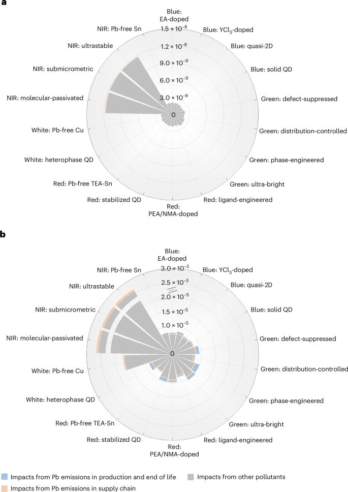
a, Terrestrial ecotoxicity attributed to Pb and non-Pb chains. b, Human non-carcinogenic toxicity attributed to Pb and non-Pb chains. The ordinate section between 2.0 × 10⁻⁵ and 2.5 × 10⁻³ is omitted for clarity. Endpoint categories include ecosystem quality (species yr–1) and human health (disability-adjusted life years). Pb emissions in the Pb-free PeLED supply chains originate from preceding-level substances. Supplementary Fig. 14 details all key processes and pollutants.
Towards commercially sustainable PeLEDs
Effective mitigation of environmental impacts
Building on the preceding lab-scale device assessments, we now simulate the life-cycle impacts of future large-scale PeLEDs by incorporating industrial techniques. These techniques include reusing organic cleaning solvents, replacing spin coating with vapour deposition, recycling metal electrodes and indium tin oxide (ITO) glass substrates, managing waste and substituting Au electrodes (in NIR devices) with less-impactful metals. Detailed descriptions of these techniques are in Methods. Industrial fabrication techniques for substrate cleaning, such as ultrasonic and pressure-gun washing, yield comparable environmental impacts, as shown in Supplementary Fig. 17. Therefore, we use the ultrasonic technique as a representative case. On the basis of the simulated industrial LCIs in Supplementary Appendix B, we illustrate the environmental benefits of individual scenarios and their combination (Fig. 4a,b). Reusing organic cleaning solvents can reduce environmental impacts by nearly 60% for most PeLEDs. Recycling metal electrodes offers minimal benefits for RGB and white devices (using Al) but is advantageous for NIR devices (using Au). Notably, replacing Au with less-impactful metals (for example, Al, Cu or Ni) significantly mitigates the impacts of NIR PeLEDs, reducing them by three orders of magnitude. While vapour deposition minimizes raw material waste, its overall environmental benefits are less pronounced due to the high energy consumption of the evaporation system. Recycling ITO glass substrates and managing waste collectively provide around a 10% reduction in environmental impacts. Some deviation between our simulations and future industrial practices is inevitable due to challenges in accurately modelling industrial techniques. However, this deviation can be narrowed as industrial parameters become more accessible. Overall, future industrial PeLEDs are projected to reduce environmental impacts by 50–90% compared with lab-scale PeLEDs. Among the six industrial techniques, controlling cleaning solvents and Au electrodes emerges as the most effective strategy for mitigating environmental impacts, supplemented by large-scale fabrication, substrate recycling and waste management.
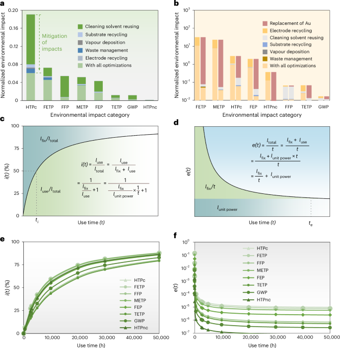
a,b, Environmental benefits of industrial techniques for RGB PeLEDs (a) and NIR PeLEDs (b). The NIR PeLED values are presented on a logarithmic scale. c, Model of the internal relation function i(t) for a power-consuming product, where Ifix represents the environmental impacts already embedded in the production, distribution and end-of-life stages, and Iunit power is a constant determined solely by the type of energy supply. d, Model of the external relation factor e(t) for a power-consuming product. e,f, Calculated values of i(t) (e) and e(t) (f) for an industrial PeLED powered by the 2020 European electricity mix.
Assessing sufficient lifetime
Lifetime is a crucial parameter for any device. While a longer lifetime is desirable, it is essential to establish an indicator that quantifies the expected sufficient lifetime. For photovoltaic devices, energy-payback time is widely used8,21. However, evaluating the break-even point between time and impact for LEDs is challenging since they consume energy during use. Here we propose a new parameter—RIMT—to determine the sufficient lifetime of electricity-consuming devices from a life-cycle perspective. RIMT represents the minimal time required to mitigate relative impacts, considering internal and external relative impacts simultaneously. The internal relative impact refers to the proportion of dynamic growth impact (during the use stage, denoted as Iuse) to the total impact (Itotal), which also includes the fixed impacts already incurred (production, distribution and end-of-life stages, denoted as Ifix). This can be described using the internal relation function:
where Iunit power represents the impact of power consumption per unit of time, and t is the real usage time. The fixed impacts become relatively minor when the dynamic growth portion predominates after a specific time point ti (Fig. 4c). The external relative impact refers to the total average impact of a device during use, described by the external relation function:
A longer use time reduces the average fixed impact during the use stage. From a specific time point te, the average impact stabilizes at a low level (Fig. 4d). Ultimately, the RIMT can be determined as the maximum of ti and te:
To illustrate this, we present an example of an industrial PeLED powered by the European electricity mix in 2020 (Fig. 4e,f). In this example, i(t) and e(t) reach favourable values when approaching 7,000–14,000 hours and 2,000–5,000 hours, respectively. Consequently, the RIMT is estimated at approximately 7,000–14,000 hours. For a projected European mix in 2050, the RIMT shifts to 6,000–22,000 hours, attributed to the gradual replacement of fossil fuels with cleaner energy sources that exhibit lower environmental impacts over time. Comparisons across energy sources and regions (Supplementary Figs. 20–30) reinforce this conclusion. For example, France, with its nuclear-dominant mix, exhibits significantly longer RIMTs than the United States, which relies heavily on fossil fuels. Overall, comprehensive assessments across various electricity scenarios indicate that RIMTs generally fluctuate around the 10,000 hour level (Supplementary Tables 40–42). We recommend future PeLEDs achieve lifetimes exceeding this threshold under typical operating conditions to mitigate the relative environmental impacts of their production.
Future commercial potential
To gauge commercial competitiveness, we evaluate the environmental impacts of several commercial technologies and compare them with PeLEDs (Fig. 5a,b, Supplementary Tables 36–39 and Supplementary Fig. 19). Current commercial technologies include III-V LEDs (for example, gallium nitride (GaN)), compact fluorescent lamps (CFLs) and incandescent lamps for lighting, as well as liquid-crystal displays (LCD) and organic LEDs (OLEDs) for displays, with quantum-dot LEDs also emerging. For lighting applications, the environmental impacts of PeLEDs are an order of magnitude lower than those of GaN LEDs and CFLs. This is due primarily to the high energy consumption required for GaN crystal growth, cutting and polishing, as well as the substantial raw material consumption for CFL production22. Incandescent lamps perform worse and are excluded from this comparison. Among display technologies, liquid-crystal displays exhibit the most severe environmental impacts across all categories, due primarily to the extensive material usage in constructing multiple thick layers23. CdS-based quantum-dot LEDs also have one to two orders of magnitude higher environmental impacts than PeLEDs because of the extensive use of organic monomers to synthesize quantum dots24. While variations in assessment accuracy exist due to differences in system boundaries and commercial confidentiality, it is evident that PeLEDs and OLEDs exhibit the best environmental performance among mainstream technologies. The preceding primary data are sourced from previous reports22,24,25,26, while the comparison of the NIR scenario is inaccessible due to the lack of reported data.
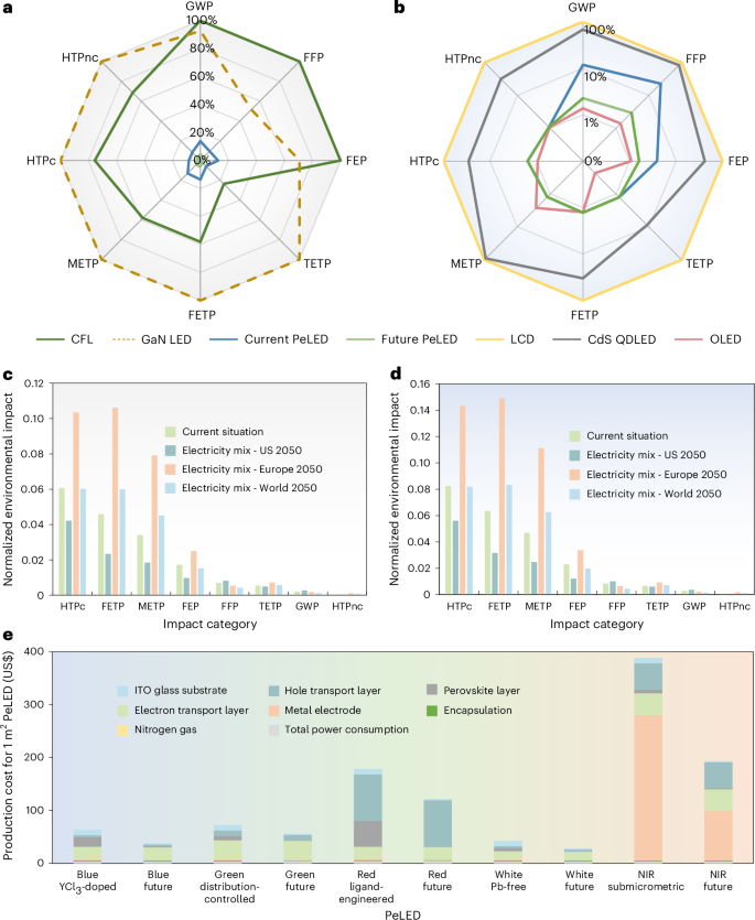
a, The environmental impacts of various lighting technologies across their complete life cycles, assuming 8,000 hours of operation with a continuous 900 lumen output during the use stage. Note that current PeLEDs have not yet achieved the technical benchmark of 900 lumens for 8,000 hours, whereas GaN LEDs can last significantly longer (exceeding 20,000 hours). Consequently, the equivalent environmental impacts of GaN LEDs in this scenario could be overestimated by up to three times. b, The environmental impacts associated with the production and end-of-life stages of various display technologies, excluding the use stage due to ongoing advancements and uncertainties in the luminous power efficiency of emerging LEDs. The values for display technologies are presented on a logarithmic scale. Across all lighting and display technologies, the comparison focuses exclusively on the light-emitting components, excluding patterning, backplane and packaging. c, The environmental impacts of future PeLEDs under various electricity mixes, excluding the use stage. d, The environmental impacts of future PeLEDs under various electricity mixes, including the use stage. e, The standardized device costs of various 1 m2 PeLEDs with a 50% active area. ITO and glass are typically sold as an integrated product, functioning as both the anode and substrate. Future NIR devices are assumed to employ recyclable Au electrodes.
The electricity mix notably influences the environmental footprint of power-consuming electronic devices. We model the environmental impacts of future PeLEDs under varying electricity mixes across different regions and periods, including current European mixes and projected mixes for Europe, the United States and the world in 205027,28,29,30. The impacts vary with different electricity inputs (Fig. 5c,d). In Europe, the dominance of wind and solar power is expected to reduce carbon footprint and most environmental impacts although it may increase toxicity due to non-ferrous metal usage and wastewater treatment. By contrast, US reliance on natural gas is expected to result in opposing trends, with higher greenhouse gas emissions but lower toxicity28,31. Globally, the environmental impacts are expected to fall between these regional scenarios. Despite these variations, the environmental performance of PeLEDs remains encouraging.
Accounting for production costs is essential for market competitiveness. Using LCIs, we estimate the production costs of current lab-scale PeLEDs and future industrial-scale PeLEDs (Fig. 5e and Supplementary Tables 43–48). The active emissive area is assumed to occupy 50% of the total area, while this proportion can increase in practice32,33. Although the electricity prices differ in different regions, the difference is insignificant as electricity contributes to a relatively small proportion of the total cost. The standardized device cost of current RGB PeLEDs varies between US$63 and US$178 m–2, with cost mainly from the charge transport materials. NIR PeLEDs exhibit a higher device cost of approximately US$388 m–2 due to the use of Au electrodes. Recycling the ITO substrate and employing large-scale deposition could reduce the industrial RGB PeLEDs’ device cost to US$38–121 m–2, which is lower than the cost of various OLEDs (US$87–265 m–2)34, excluding control backplanes for both PeLEDs and OLEDs. Assuming other costs (for example, depreciation and labour) are comparable to those of commercial OLED panels35, the total cost of a future industrial RGB PeLED product is estimated to be in the vicinity of US$100 m–2. Although determining precise cost values remains challenging and is not the focus of this study, our techno-economic assessment results highlight the remarkable economic potential of PeLEDs.
Discussion
We present a comprehensive overview of the environmental impacts, economic costs, and potential industrial advancements of emerging PeLED technology, employing a cradle-to-grave life-cycle assessment for various PeLEDs. This study focuses exclusively on the light-emitting components, omitting the patterning and backplane, which are required for practical applications. Although the inclusion of patterning and backplane would elevate the normalized environmental impact values, such increases are not unique to PeLEDs but are consistent across other LED technologies. We also recognize the inherent challenges and limitations of conducting analyses on pre-commercial technologies, where manufacturing processes remain unestablished. Consequently, this work does not aim to assert the precision of the numerical findings but rather to provide a rational and qualitative framework for guiding the sustainable commercial development of PeLEDs.
In the pathway to sustainable commercialization, environmental, economic, and technical factors emerge as three critical pillars that align the interests of key stakeholders: the coordinator (government legislation and policy), producers (corporate profitability and return on investment), and customers (willingness to pay). Our findings suggest that future PeLEDs developed through large-scale manufacturing, hold great promise in achieving competitive standing among various lighting technologies from both environmental and economic perspectives. Notably, due to the thin emissive layer, measuring only tens of nanometres, the contribution of Pb in PeLEDs to overall environmental impact is minimal. From a technical standpoint, achieving a device lifetime of the order of ten thousand hours is a practical target to offset relative environmental impacts. Furthermore, luminous power efficiency deserves further attention to advance the energy efficiency classification of future PeLED products.
Methods
Investigation of PeLED devices
The selected 18 PeLEDs demonstrate high technical performance and are widely recognized. The technical specifications of a PeLED device, including thickness, mass, material consumption and fabrication equipment, are detailed in the Supplementary Appendices. Materials for the PeLED devices are acquired or retrieved from chemical companies such as Sigma-Aldrich, Thermo Scientific, TCI Europe and Ossila unless stated otherwise.
Goal and scope definition
Unless otherwise specified (for example, in the commercial comparison or LCIs), the functional unit for all 18 PeLEDs and future PeLEDs is set as 1 m2. The normalized life-cycle impact values for this 1 m2 PeLED can be directly proportioned for differently sized products. The LCA is conducted using this quantification benchmark. The system boundary encompasses all steps from the material synthesis of perovskites to device assembly. The five life-cycle stages are illustrated in Fig. 1. The raw material acquisition stage encompasses the input of all direct and indirect raw materials within the boundary, including the preparation of ITO glass substrates, production of hole and electron transport layers, synthesis of perovskite materials, production of perovskite thin films, cathode deposition and device encapsulation. Manufacturing involves the production of functional PeLED devices, where electricity consumption and direct waste emissions are significant inputs and outputs. The origins of raw materials and equipment can be traced back to earlier references cited in the Supplementary Information. The distribution stage considers primarily transport, with consumption and emissions evaluated on the basis of previous studies. During the use stage, PeLED devices are employed primarily in display or lighting applications, considering only electricity consumption. At the end-of-life stage, disposal involves either landfilling or partially recycling materials10,20.
LCI acquisition
LCA data acquisition typically requires LCI data and a secondary database. The LCI data in this study include raw materials consumption, energy input, waste discharge, recycling or landfill of devices and transport (assuming 100 km by truck). For the raw materials acquisition stage, material consumption quantities were measured by mass on the basis of experimental data aligned with documented recipes. Energy consumption and emissions during manufacturing were calculated using laboratory data or literature. In the use stage, energy consumption is influenced by factors such as luminous power efficiency, brightness, product area, use duration and energy efficiency class, as shown in Supplementary Figs. 1–3 and Supplementary Tables 6 and 7. Proportions of discarded or recycled components and materials are derived from previous studies20,36,37,38 and simulations (Supplementary Figs. 16–18). Inputs and emissions during raw material production, transport, waste treatment and energy generation are sourced from the secondary database Ecoinvent14. Emission factors for most raw materials, including electricity generation, deionized water, ITO, acetone, toluene, methyl acetate, chloroform, Au and Al, are extracted from Ecoinvent. For non-commercialized chemicals not covered by Ecoinvent, including poly[bis(4-phenyl)(2,4,6-trimethylphenyl)amine], methylammonium bromide, formamidinium iodide, lead bromide and lead iodide, LCIs from perovskite photovoltaic studies8,9,10 are used, supplemented by literature and chemical property considerations24,34,39. Additional adaptations for similar substances are detailed in Supplementary Table 9.
Life cycle impact assessment and interpretation
Life cycle impact assessment links inventory data to various environmental impact categories by applying characterization factors (CFs). A pre-assessment (Supplementary Fig. 4) identified key impact categories, with the primary focus on global warming potential, fossil fuel potential and toxicity-related categories (human carcinogenic toxicity, HTPnc, terrestrial ecotoxicity, freshwater ecotoxicity and marine ecotoxicity). Global warming potential CFs are derived from the Intergovernmental Panel on Climate Change (IPCC) method40, while other CFs are sourced from the ReCiPe 2016 Midpoint model, which is constructed on the Eco-indicator 99 and CML (Institute of Environmental Sciences at Leiden University) model12,41,42. Fossil fuel potential is quantified by surplus cost potentials arising from resource extraction, with CFs calculated through a log-linear cumulative cost–tonnage relationship12. Cultural perspectives theory is applied in the ReCiPe model, using perspective H (hierarchies). Meanwhile, CFs of IPCC global warming select 100 years to maintain the consistency. Toxicity CFs are calculated on the basis of the USES-LCA 3.0 model, encompassing all emissions compartments (for example, urban and rural air, freshwater, seawater, agricultural and industrial soil). As large-scale commercial use of PeLEDs is not yet realized, disposal-stage data rely on theoretical assumptions and mass balance. Solid and hazardous waste emissions are modelled using landfill and incineration data from Ecoinvent. Software utilized for this section includes Microsoft Excel (version 16.83), OriginPro (2022 SR1) and SimaPro (version 9.3).
Uncertainty and sensitivity analyses
Uncertainty analysis is conducted using Monte Carlo simulations to capture the distribution of environmental impacts across different PeLEDs on the basis of the assigned distribution patterns of input parameters and secondary database14,43. Input parameters, such as lifetime, recycling rate and energy consumption, were subject to uncertainty. Consequently, we conduct a systematic sensitivity analysis by assigning a specific distribution to each parameter to determine the input parameters that contribute most to the variability of environmental impact during the PeLEDs’ life cycle (Supplementary Figs. 5 and 6 and Supplementary Tables 16–35). In addition, a mass-based allocation method is applied for life cycle impact assessment in recycling scenarios.
Simulation of industrial techniques
First, as the cleaning process involves straightforward chemical exchanges, the waste liquid of cleaning can be directly used many times without chemical decontamination. According to the industrial standard, we assume that the cleaning solvents can be reused 20 times (4 times per day), and the consumption rate is less than 1%36. Second, the ITO glass substrates can be recycled after end of life37,38. We pre-investigate the effects of different recycle times (Supplementary Fig. 16), where five recycle times of glass substrates is considered reasonable20. Third, we upgrade the deposition process from spin coating to vapour deposition, thereby enabling a low liquid waste emission (for perovskites and hole transport layers) and recycling unused materials (for metal electrodes) with a specific recycling rate. Fourth, waste management refers to reasonable recycling or landfills for other components based on previous investigations10,20. Fifth, less-impactful metals are likely to replace Au as electrodes for NIR devices in the future. In this work, we assess Ni, Cu and Al as examples44,45,46.
Techno-economic assessment
Techno-economic assessment is performed to complement the LCA of PeLEDs and determine the costs and cost savings through different industrial techniques. A cradle-to-gate scope is chosen, taking the perspective of the manufacturer. Hence, the calculation is limited to accounting for raw material and electricity use during the device assembly without including the cleaning costs (consistent with previous reports). The quantity of materials and electricity used are the same as in the preceding sections, such as the LCI and details of industrial techniques. The industrial techniques introduce reduced quantities of selected materials considering closed-loop recycling. The corresponding costs of materials are based on the bulk supply prices provided by chemical companies, while the electricity prices consider both the 2022 United States and Europe for industrial consumers.
Reporting summary
Further information on research design is available in the Nature Portfolio Reporting Summary linked to this article.


Responses