Ultra-low-power consumption silicon electro-optic switch based on photonic crystal nanobeam cavity

Introduction
Silicon photonics integration1 attracts interest due to its many advantages, such as a compact footprint and compatibility with complementary metal–oxide–semiconductor (CMOS) process technology. These features have led to expectations that silicon-based integration will replace traditional parallel electrical links and meet the future bandwidth, density, cost, and power consumption requirements of the computing and communications industries2. Many devices on silicon platforms have been investigated, such as modulators3, switches4,5,6, mode multiplexers7, splitters8, and filters9. Among these, optical switches are critical components of data centers and high-performance computers for implementing routing, switching, and optical cross-connections10,11. To acquire these on-chip functions, optical switches are typically integrated on a large scale, often in hundreds, which presents a fundamental challenge of high power consumption12.
Silicon-integrated electro-optic (EO) switches, including Mach–Zehnder interferometers (MZI), microring resonators (MRR), and hybrid types that combines MRR and MZI, have been widely investigated. Owing to the enhanced electromagnetic energy density and smaller active material volume from the resonators13, MRRs show more efficient power consumption than MZIs. However, limited by the minimum bending radius (~5 μm) of silicon waveguides, it is challenging for MRR to further reduce power consumption by increasing the electromagnetic energy density.
A one-dimensional (1D) photonic crystal (PhC) nanobeam cavity (PCNC) offers a compact footprint14 with a wavelength-scale mode volume15. It contains Bragg mirrors in the bandgap and a resonator cavity in the energy band to form a short Fabry–Perot cavity. In PCNC, the optical field is concentrated in the center of the structure, which provides a powerful means for increasing the electromagnetic energy density to enhance the interactions between light and the material14. Unlike the MZI and MRR, which have a constant optical distribution in the waveguides, the PCNC allows precise control of the optical field within a smaller active material volume.
In this study, we present the design and experimental demonstration of an EO switch based on a PCNC-assisted MZI. In the simulation, we confined the light in a small mode volume of 0.12 μm3, enabling us to tune the resonant wavelength by plasma dispersion effect in a 10 μm silicon waveguide length. The fabricated device shows an ultra-low static power consumption of 0.10 mW, a compact footprint of 18 μm × 200 μm, and a fast EO switching time of 0.43 ns and 1.27 ns. The PCNC was designed with a reasonable Q factor of approximately 5000 to enable sufficient optical bandwidth to support high-speed data transmission. Higher-Q-factor resonant cavities require less power for state switching (a smaller blue shift is required). However, this sacrifices the available optical bandwidth, resulting in a lower data transmission rate. In this study, we made a trade-off between power consumption and transmission data rate. The insertion loss (IL) and crosstalk (CT) of the switch were measured as 1.04 dB and −19.48 dB in the cross state (0 mW), and 1.06 dB and −11.85 dB in the bar state (0.10 mW), respectively. In the dynamic working state, the switching power is calculated to be only 6.34 fJ/bit. Moreover, we performed a 136-Gb/s four-level pulse amplitude modulation (PAM-4) signal transmission experiment to verify the capability of the proposed EO switch to support high-speed data transmission. The proposed device has the lowest static-tuning power consumption among silicon EO switches and the highest transmission data rate. This study demonstrates the potential applications in future high-performance optical computers, data center interconnects, optical neural networks, and programmable photonic circuits.
Results
Device design and numerical simulation
The design of the PCNC is shown in Fig. 1a. The PCNC is based on a silicon rib waveguide consisting of two mirror regions and taper regions, surrounded by silica cladding. To obtain a fundamental resonant mode in the C band, the mirror regions must ensure a photon bandgap in the region of interest (ROI). The tapered regions act as resonant cavities designed to match the effective indices of the evanescent mirror Bloch mode and waveguide mode14. The PCNC is symmetric with respect to its center. We designed the period of the mirror region to be a = 320 nm to attain a resonance peak around 1550 nm, and the width as W = 1 μm. The detailed parameters of the PCNC were optimized via simulation to the following equations:

a Structure of the PCNC. b Basic unit cell of the 1D PhC. Band diagram of the 1D PhC in the c mirror region and the d center cell. The simulated transmission and reflection spectra of the designed PCNC under e zero bias, f 0.96 V bias, and g 1.00 V bias.
Figure 1b depicts the basic unit cell of a 1D PhC, and the band diagram is shown in Fig. 1c for the mirror regions simulated using the finite element method. A bandgap of approximately 190 nm was generated at the boundary of the Brillouin zone. Figure 1d shows the band diagram of the center cell in the tapered region. Due to the smaller period, the transverse electric mode A (TE-A) covered the ROI and resonated due to the photon bandgap in the mirror region.
Next, we simulated the PCNC using a three-dimensional (3D) finite-difference-time-domain (FDTD) simulation tool. The Q factor and mode volume were optimized to be approximately 5000 and 0.12 μm3 in the simulation. The resulting mode volume was roughly one order of magnitude lower than that of an MRR with the same Q factor. The optical concentration factor was calculated to be approximately 20, according to a previously reported method in reference13. Insets (i) and (ii) in Fig. 1a show the mode profile of the input light and the optical electric distribution of the PCNC at resonance, respectively. The transmission and reflection spectra of the designed PCNC are shown in Fig. 1e. The simulated IL and extinction ratio were 0.39 dB and 21.61 dB under zero bias voltage, respectively.
Finally, we designed a switch based on the MZI architecture with two PCNCs embedded in both arms. Two 2 × 2 Multimode Interferometers (MMIs) were used to split and combine the light power at the input and output ports. Figure 2a shows the configuration of the EO switch. The two MMIs were designed using the process design kit (PDK) of AMF, with an excess loss of 0.18 dB and an imbalance of 0.07 dB. To achieve high modulation efficiency16, we designed two PIN junctions to tune the PCNCs. The change in the refractive index and absorption coefficient caused by variation in the free carrier concentration in silicon around a wavelength of 1550 nm is given by the following empirical formulas17:
where (Delta {N}_{e},,Delta {N}_{h}) are the concentration changes of electrons and holes, respectively. The cross-section of the configuration is shown in Fig. 2b. The distance between the P++ region and N++ region is set to 2 μm, balancing the drive voltage and the excess IL. When a positive bias voltage is applied, the holes and electrons in the P++ and N++ regions are injected into the intrinsic silicon waveguide region. This changes the effective refractive index of the rib waveguide by −0.0017 and −0.0025 under forward bias voltage of 0.96 V and 1.00 V, respectively. Consequently, the resonance peak of the PCNC is blue-shifted by 0.51 nm and 0.75 nm, as shown in Fig. 1f, g. Further details are provided in the Supplementary Information Section 1.
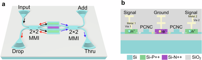
a The device configuration of the EO switch. The black arrows indicate the path of incident light, the red arrows show the path of reflected light, and the blue refers to the path of transmitted light. b Cross section of the configuration.
Four grating couplers were used to couple light onto the chip. The incident light was split into two beams with a phase difference of 90° using the first 2 × 2 MMI. When the wavelength of the light was equal to the resonant wavelength of the PCNC, the light propagated forward through the PCNCs, combined with the second 2 × 2 MMI, and then output from the Thru port. When the wavelength of the light deviated from the resonant wavelength of the PCNC, the light was reflected by the PCNCs, combined with the first 2 × 2 MMI, and then output from the Drop port.
Fabrication and characterization
The device was fabricated on a 220 nm silicon-on-insulator (SOI) platform under a standard multi-project wafer (MPW) run at an advanced micro foundry (AMF) in Singapore (see “Methods” for the details of device fabrication). The PCNC was designed on a 90 nm slab to enable the construction of the PIN junctions and tuning of the resonant wavelength. Figure 3 shows a microscopic image of the fabricated EO switch and a reference waveguide with grating couplers to normalize the transmission spectra. Due to the thick silica cladding, it was difficult to obtain detailed scanning electron microscope images of the fabricated devices. The footprint of the switch was 18 μm × 200 μm, which could be further reduced by designing a smaller 2 × 2 MMI. The active tuning length was 10 μm per arm, which was almost the same as the PCNC length. Two heaters were placed directly above the PCNC to align the two resonance peaks, but no power was applied to the proposed device.
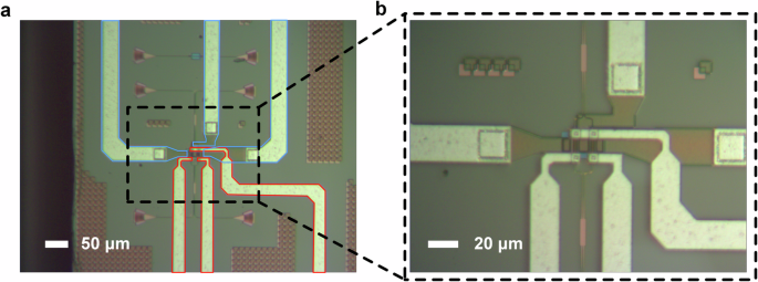
a The optical microscope image of the proposed EO switch and grating couplers. The blue line represents the aluminum wire connecting the EO electrodes, and the red line represents the aluminum wire connecting the heaters. b Zoomed-in image showing the two PCNCs at the center.
To characterize the static performance of the fabricated switch, we employed a continously tunable laser as the light source. Four grating couplers from the PDK were used to couple light into and out of the proposed switch. According to the transmission spectra of the reference waveguide, the coupling loss of the grating coupler was approximately 4 dB/facet at a wavelength of 1550 nm.
Figure 4a shows the transmission spectra of the device without any power supplied to the heaters or PIN junctions. The results indicate an initially aligned resonance peak at 1556.16 nm, with an IL and 3-dB bandwidth of 1.04 dB and 0.37 nm (~46 GHz), respectively. Then, considering the on-off characteristics of the PIN junctions, a voltage source was applied to the proposed switch through an electrical probe from 0.96 to 1.00 V in steps of 0.01 V. Electrons and holes were squeezed into the PCNC, resulting in a decrease in the refractive index and an increase in the absorption coefficient of silicon. Consequently, the resonance peaks of both PCNCs were blue-shifted with decreasing Q factor and increasing IL.
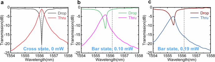
a The initial transmission spectra with an aligned resonant peak. b Measured transmission spectra under a 0.96 V forward bias. c Measured transmission spectra under a 1.00 V forward bias.
As shown in Fig. 4a, the carrier wavelength was set to match the resonance peak at 1556.16 nm, thus the EO switch initially worked in the cross state. The IL and CT were 1.04 dB and −19.48 dB, respectively. When a voltage of 0.96 V was applied to both PIN junctions, the resonance peak blue-shifted to 1555.68 nm, corresponding to a static power consumption of 0.10 mW. Meanwhile, the device switched to the bar state, with an IL and CT of 1.06 dB and −11.85 dB, as shown in Fig. 4b. Furthermore, when the applied voltage was increased to 1.00 V, the IL and CT of 0.79 dB and −15.11 dB were obtained with the resonance peak blue-shifting to 1555.42 nm, as shown in Fig. 4c. Due to the exponential increase in the PIN junction current, the static power consumption increased to 0.19 mW. The experimentally observed resonant wavelengths were less blue-shifted compared to the simulation results in Fig. 1e–g. This discrepancy arises because the heat generated by free carriers flowing through the nanobeam increases the effective refractive index of the waveguide, counteracting the carrier dispersion effect.
Additionally, an on-off switching test was performed to characterize the dynamic performance of the switch device. We loaded the square-wave electric signals with an amplitude of −1 V to 0 V at 50 MHz onto the two PIN junctions through a GSG probe. The driving square wave and the output signals from the PD are shown in Fig. 5. The switch demonstrated a 10–90% rise time of 0.43 ns and a fall time of 1.27 ns (More details are discussed in Section 2 of the Supplementary Information). Moreover, the capacitance of the PIN diode is calculated to be 27.5 fF and 30.1 fF at 0.96 V and 1.00 V bias, corresponding to a switching power of 6.34 fJ/bit and 7.53 fJ/bit, respectively, using the well-known (frac{1}{4}{{rm{CV}}_{{pp}}}^{2}) formula.
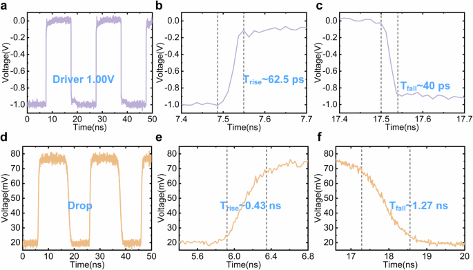
a The applied square-wave driving signal, b the rising edge, and c the falling edge. d The output signal from the Drop port, e the rising edge, and f the falling edge.
High-speed transmission experimental setup
To investigate the transmission performance of the proposed EO switch, we measured the BER of the switch with a 136-Gb/s PAM-4 signal, which is the highest reported rate for a 2 × 2 silicon EO switch. The experimental setup and transceiver DSP flows are shown in Fig. 6a–c and described in detail in the “Methods” section. Figure 6d shows the BER performance of the 68-GBaud PAM-4 signal in the presence of optical switching at the Drop and Thru ports. The BERs of the signal output from the Drop and Thru ports were below the 7% forward error correction (FEC) threshold. Compared to the optical back-to-back (OBTB) sensitivity of −18.5 dBm at the BER threshold, negligible penalty was observed for the Drop port, which indicates that the bandwidth of the proposed switch was wide enough for the high-capacity switching at 136 Gb/s. However, the Thru port exhibits a penalty of 5.5 dB due to its limited bandwidth. Insets (i)–(iv) provide the recovered eye diagrams at −8-dB ROP in different conditions. The high-speed transmission experiment unambiguously demonstrated that the proposed EO switch can be used in on-chip optical communication.
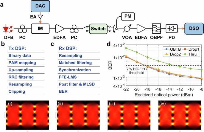
a Experimental setup of the 136-Gb/s transmission. b, c Transceiver DSP flow charts. d BER versus received optical power. Insets (i)–(iv): recovered eye diagrams at −8-dB ROP in OBTB, Drop1, Drop2, and Thru conditions, respectively. PM power meter, Drop1 Drop port under 1 V forward bias, Drop2 Drop port under 0.96 V forward bias.
Discussion
In summary, we designed and experimentally demonstrated an ultralow-power-consumption EO switch on a standard SOI platform. The PCNC structure was used to confine the light in a small mode volume of 0.12 μm3 in the simulation. As a result, an ultralow static power consumption of 0.10 mW and a dynamic switching power of 6.34 fJ/bit was achieved, while supporting a high-speed 136-Gb/s PAM-4 signal transmission. The experimental results also indicate a switching time of 0.43 ns and 1.27 ns. The two PCNCs were aligned in the initial state, benefiting from the precision of the fabrication; thus, thermal tuning was not required. However, in large-scale integration, thermal tuning for wavelength alignment is necessary due to fabrication errors, which introduces additional power consumption. A summary of previously reported integrated EO switches on the SOI platform is provided in Table 1. The proposed switch demonstrated the lowest static power consumption and the highest data transmission rate when the two PCNCs were aligned in the initial state. The switch was fabricated under an MPW run at the AMF, which is compatible with a mature CMOS process. By arranging a series of switch units in a topology, switch arrays of varying scales can be attained to meet the requirements of different application scenarios. This study attains an ultralow-power-consumption silicon EO switch with balanced performances in the IL and CT, showing potential for high-density integration and future high-performance applications.
Methods
Numerical simulation
The transmission spectra, Q factor, and mode volume of the PCNC were simulated and optimized using a 3D FDTD tool (Lumerical FDTD solutions) with perfectly matched layer boundary conditions.
Device fabrication and characterization
The device was fabricated on a 220 nm SOI platform under a standard MPW run at AMF in Singapore. The platform provided three etch depths to define the grating couplers, slab waveguides, and strip waveguides using three mask layer processes. The grating couplers and slabs were protected by a photoresist to prevent additional silicon etching during the grating coupler and slab processes. Eight implantations were performed on the high-speed modulators and Germanium (Ge) photodetectors. The doping concentrations of P++ and N++ were estimated to be 1 × 1020 cm−3 and 1.5 × 1020 cm−3, corresponding to sheet resistances of 160 Ω/□ and 60 Ω/□, respectively, provided by AMF. Additionally, two metal layers and vias were used for electric connections. The static EO performance of the fabricated switch was characterized using a tunable laser (Keysight 81960A), an optical power meter (Keysight N7744A), and a source meter (Keithley 2400). To demonstrate the EO tuning process, a DC probe was used to connect the source meter and electrodes to apply different voltages. Additionally, an on-off switching test was conducted to characterize the dynamic performance of the switch. A ground-signal-ground (GSG) probe was used to load the 50 MHz square-wave electric signals onto the two PIN junctions.
High-speed transmission experimental setup
Here, we detailed the transmission performance through the Drop and Thru ports at 1556.16 nm for both Bar and Cross states. The experimental setup for the 136-Gb/s PAM-4 signal transmission is shown in Fig. 6a. The electrical signal was generated with a 100-GSa/s digital-to-analog converter (DAC), (Micram DAC4) and amplified using an electrical amplifier (EA). The signal drives a 25-GHz intensity modulator (IM) with a quadrature bias. A distributed feedback (DFB) laser was used as the light source, followed by a polarization controller (PC) to align the polarization states between the laser and the IM. After being boosted by an erbium-doped fiber amplifier (EDFA), the modulated PAM-4 signal entered the silicon chip, and the polarization state was adjusted by another PC. At the output of the silicon chip, the received optical power (ROP) was varied using a variable optical attenuator (VOA), followed by an EDFA to compensate for the loss and an optical bandpass filter (OBPF) to filter out the amplified spontaneous emission noise. Finally, the optical signal was detected with a 70-GHz photodetector (PD) and captured using a 160-GSa/s digital storage oscilloscope (DSO, LeCroy 59Zi-A). The transceiver digital signal processing (DSP) flow charts are shown in Fig. 6b, c. On the transmitter side, the PAM-4 signal is up-sampled and pulse-shaped by a root-raised-cosine (RRC) filter with a roll-off factor of 0.01. After resampling and clipping, the PAM-4 signal was loaded into the DAC. On the receiver side, the signal was resampled and match-filtered. After frame synchronization, a least-mean-square (LMS) algorithm-based linear feedforward equalizer (FFE) was applied for channel equalization. To suppress the enhanced in-band noise caused by linear equalization, we used a two-tap post filter cascaded with the maximum-likelihood sequence decision (MLSD). Finally, the bit error rate (BER) was calculated to evaluate the performance.


Responses