Ultra sensitive low-frequency visible light dielectric response measured by real capacitance method

Introduction
Capacitors are one of the key components of modern electronic products, widely used in various fields such as electronics, power, and energy storage. As an indispensable key component in capacitors, the physical properties of dielectric materials directly determine the performance of capacitors1,2. At present, the existing dielectric materials can no longer meet the actual needs of the electronic industry application requirements urgently require the development of new dielectric materials with better performance, as well as new functional dielectric materials with controllable light, sound, and magnetic properties3. In recent years, photo-induced phase transition has been increasingly applied in material research, and significant achievements have been made in fields such as photo-induced magnetism, neutral ion valence state changes, and spin crossover transitions4,5,6,7. These photo-induced macroscopic phases are not derived from thermal effects but are caused by the synergistic effect between spin, dipole, and lattice distortion in photo-excited states8. The study of this mechanism has always been one of the most exciting frontiers in materials science and condensed matter physics exploration.
The change in dielectric constant caused by light can be called the photo dielectric effect (PDE), which was discovered on the phosphor of the ZnS-CdS type in 19099. Since then, many meaningful works have been reported. These research works mainly focus on sulfides10,11, quantum paraelectrics12,13,14,15,16, and other dielectric materials17,18,19,20,21,22,23,24,25. The standard dielectric characteristic measurement uses the capacitor method, which means that both sides of the sample are electrodes. However, measuring the optical dielectric properties involves the transparency of the electrode and the sample itself. Therefore, PDE is related to the lighting method of the sample to be measured. The earliest optical dielectric measurement was achieved by compressing an average 0.1 mm thick powder layer of the measured sample between transparent electrode plates11. However, the air spaces among the powders affect the measurement effect, and less adopted in the latter.
For bulk samples, due to the difficulty in making transparent conductive electrodes, there are usually three methods for optical dielectric measurement. Firstly, for transparent or semi-transparent samples, two measuring electrodes on the same side with light shining from the other side13, as shown in Supplementary Fig. S1a; Secondly, for the opaque sample, two measuring electrodes on the same side with light shining from the same side12, as shown in Supplementary Fig. S1b; These two methods are called Unreal capacitance measurement (URCM) because there is no sample between the two electrodes facing each other. In order to increase the rate of change in the dielectric constant, the thickness of the sample for the PDE measurement is generally 0.2–0.5 mm12. Using the URCM method, the marked photo-induced enhancement of a static dielectric constant has been reported in quantum paraelectric SrTiO3 and KTaO3, in which photoconduction is subsequently considered the main mechanism causing giant PDE among several mechanistic explanations12,13,14,15,16. However, these giant PDEs occur at temperatures below 50 K or even at 5 K, with the assistance of large bias voltages or strong UV light irradiation, making them difficult to apply in practice. Although a large rate of change in dielectric constant can be measured, the URCM method mainly measures the surface dielectric response and is not suitable for non-uniform electrolytes or even oriented uniform electrolytes. Thirdly, the real capacitance measurement method (RCM) has been widely adopted in recent years, with two transparent or semi-transparent electrodes on opposite sides forming a true capacitance, and light shines from one side, as shown in Supplementary Fig. S1c. In the RCM method, even if the sample is as thin as a few tenths of a millimeter, for opaque one, the rate of change in the dielectric constant of light modulation is usually very small due to the limited light penetration thickness. Therefore, the thickness of the sample for the PDE measurement is generally 0.2–0.3 mm18,19,20,21,22,23. Many excellent PDE works have been reported successively17,18,19,20,21,22,23. However, in these reports, only ultraviolet light can better stimulate strong PDEs. Despite many attempts at visible light PDEs, the dielectric changes in the visible light region are very small due to the large bandgap of these materials24,25.
SmCrO3, as a typical multiferroic material, shows exotic antiferromagnetic (AFM) and ferroelectric (FE) properties26. In Tauc’s plots of the SmCrO3 compound, two prominent peaks are observed around 466 nm and 690 nm which are attributed to the transitions of O2p–Cr3dt2g and Cr3dt2g–Cr3deg due to octahedral crystal field splitting of d-orbitals. These transitions correspond to the bandgap energies of 2.7 eV and 1.9 eV, respectively27, indicating the possibility of visible light modulation of the physical properties of SmCrO3. In this work, we used the RCM method (inset of Fig. 2d) to observe Maxwell–Wagner type relaxation and Debye type relaxation peaks modulated by visible light in 1.0 mm thick SmTixCr1−xO3 (x = 0, 0.05, 0.1, 0.2) samples. A maximum of +790% ultrasensitive low-frequency photo-dielectric variation was observed in SmTi0.05Cr0.95O3 sample and visible light can also modulate the appearance of Debye relaxation peaks.
Results and discussion
SmTixCr1−xO3 (x = 0, 0.05, 0.1, 0.2) samples were synthesized by solid-state reaction method. X-ray diffraction (XRD) (Supplementary Fig. S2), Rietvled-refined XRD patterns (Supplementary Fig. S3), The lattice parameters of the samples (Supplementary Table S1), Variation of primitive unit cell parameters and volume against titanium content (Supplementary Fig. S4), X-ray photoelectron spectroscopy (XPS) (Supplementary Fig. S5), and magnetic properties (Supplementary Fig. S6) all confirmed that the B-site doping of Ti was successful. In Fig. 1, (varepsilon ^{prime}) of SmCrO3 sample is larger than 104 at low frequency above 200 K. Under an external AC electric field, the hopping motion of the localized holes gives rise to dipolar effect and sizable polarization which are responsible for the large values of the constant at high temperature28. The giant low-frequency dielectric constant, with step-wise dependence on temperature and strong dependence on frequency, is a clear signature of dielectric behavior being dictated by regions of different conductivity, which can be well described by the Maxwell–Wagner model29,30. Anomalously, after Ti doping, the dielectric constant of SmTixCr1−xO3 decreases in order of magnitude, as shown in Fig. 1b. The peak temperature of the loss tangent and the thermal activation temperature significantly increased with the increase of Ti content (as shown in Fig. 1c, d), but the loss tangent did not show a significant change. Remarkably, the electrical resistivity of SmCrO3 at room temperature is about 4000 Ω·m, which is still a semiconductor. After Ti doping, the room temperature electrical resistivity approaches 107 Ω·m and in order of magnitude increases with the increase of Ti content, becoming an insulator, as shown in Fig. 1e.

a SmCrO3 sample. b SmTi0.05Cr0.95O3 sample. c SmTi0.1Cr0.9O3 sample. d SmTi0.2Cr0.8O3 sample. e the resistivity measured at a frequency of 100 Hz and a voltage of 0.5 Ṽ.
For pristine SmCrO3 samples, as shown in Fig. 2a, the dielectric constant decreases with increasing frequency under both dark and light conditions. Surprisingly, in the low-frequency range, light causes the dielectric constant to decrease (see inset of Fig. 2a), while in the high-frequency range, it increases. This abnormal phenomenon, which has not been reported yet, was reproduced in the re-prepared sample (see Supplementary Fig. S7). Using segmented measurements from 20 to 1000 Hz and from 1000 Hz to 1 MHz, it has been proven that this is a reproducible non-accidental phenomenon (see Supplementary Fig. S8). The rate of change of dielectric constant shows a negative and then positive change with frequency, with a minimum value exceeding −46% at 100 Hz (measure voltage 0.5 Ṽ) and a maximum of nearly 654% peak around 8 kHz. The curves of loss tangent with frequency exhibit typical WG relaxation behaviors under dark and light conditions, in which the loss peaks appeared in the high-frequency range, and the loss increased with the decrease of frequency in the low-frequency range. The loss tangent curve under illumination seems to be a shift of the loss tangent curve in the dark towards higher frequencies. The real part of the Cole-Cole plot confirms that the dielectric constant decreases by about half under illumination, while the imaginary part reflects a significant increase in loss.
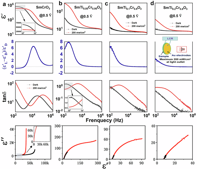
a SmCrO3 sample. b SmTi0.05Cr0.95O3 sample. c SmTi0.1Cr0.9O3 sample. d SmTi0.2Cr0.8O3 sample.
For the B-site Ti-doped SmTi0.05Cr0.95O3 sample, as shown in Fig. 2b, the dielectric constant decreases with increasing frequency under both dark and light conditions. In the low-frequency range, the dielectric constant increases sharply under illumination. The rate of change of the dielectric constant shows a maximum peak of 790% at low frequencies and sharply decreases to only about 4% at 1 MHz with increasing frequency. Corresponding to a sharp change in the optical dielectric constant, loss tangent exhibits a Debye relaxation peak. Valuably, loss tangent is smaller under illumination and even smaller in the low-frequency range than in darkness (see inset of Fig. 2b). For the SmTi0.1Cr0.9O3 sample, the optical dielectric constant still significantly increases in the low-frequency range (Fig. 2c), and the rate of change of the dielectric constant under 100 Hz illumination is as high as 653%. The loss tangent also shows a Debye relaxation peak under illumination. For the SmTi0.2Cr0.8O3 sample, the optical dielectric constant still significantly increases (Fig. 2d), and the rate of change of the dielectric constant under 100 Hz illumination is as high as 258%. The loss tangent also shows a broad Debye relaxation peak under illumination. The Cole-Cole plots of the three doped samples also reflect a significant increase in dielectric constant, while the loss does not increase synchronously.
Unlike previous optical dielectric experiment samples with a thickness of 0.2–0.4 mm, the samples here are all 1.0 mm thick and still exhibit hypersensitive optical dielectric response at low frequencies. As can be seen in Fig. 3a, all the samples showed significant light absorption in the measurement range of 300–900 nm, with the absorption exceeding 70% in both the UV and visible ranges. Especially in the pure SmCrO3 samples, the absorption remained between 72% and 75% in the whole measurement range. The absorption curves of the SmTi0.05Cr0.95O3 samples were basically the same as those of the original samples, but the absorption in the infrared range was obviously reduced to about 72%. As the doping amount of Ti increases, the absorption of light in the infrared region weakens, but it actually becomes stronger in the ultraviolet and visible light ranges. The pristine sample has bandgap energies of 2.7 and 1.9 eV, but from the perspective of light absorption rate, these samples can all exhibit high absorption in the full spectrum, indicating that there may be many defects in the samples that capture charge carriers and form localized states. The curves converted by the Tauc equation are drawn in the inset of Fig. 3a, and the bandgaps of SmTixCr1−xO3 (x = 0, 0.05, 0.1) and SmTi0.2Cr0.8O3 are about 1.64 eV, 1.89 eV, respectively. The decrease in bandgap may be due to the formation of oxygen vacancy defects during high-temperature sintering. The formation of oxygen vacancies will create a void with a dangling bond on the adjacent metal ions so that the charge is concentrated around the vacancy and the bandwidth is reduced31. As shown in Fig. 3b, under the action of three monochromatic light sources of 405, 785, and 905 nm at 200 mW/cm2, the changes in dielectric constant and loss are almost identical, and there is no dependence on optical frequency. Under the action of three different intensities of light: 50, 150, and 200 mW/cm2, the variation of the optical dielectric constant increases with the increase of light intensity, while the loss tangent does not increase obviously. However, the loss peak shifts towards higher frequencies with the increase of light intensity, indicating a dependence on light intensity, As shown in Fig. 3c.
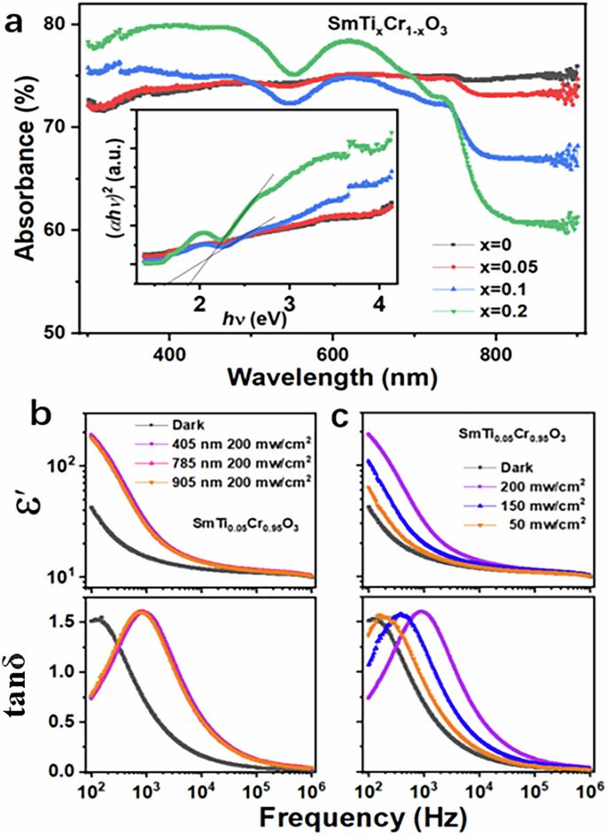
a Absorption spectrum, inset is Tauc’s plots of the samples. b SmTi0.05Cr0.95O3 sample under dark and monochromatic light irradiation with three different frequencies and the same energy density. c SmTi0.05Cr0.95O3 sample under dark and visible light irradiation with three different intensities.
In Fig. 4a, under both darkness and illumination, the dielectric constant decreases with the increase of the measured voltage, and the magnitude of the decrease is greater in the dark state. So the rate of change of dielectric constant under illumination gradually decreases in the negative direction with the measured voltage, and the maximum negative value exceeds −51% at 0.1 Ṽ, as shown in the inset of Fig. 4a. The dielectric loss increases with the increase of the measured voltage, and the magnitude of the increase is greater under illumination. The samples doped with Ti (only SmTi0.05Cr0.95O3 and at 100 Hz here), within the variable range of measured voltage, exhibit no obvious change in dielectric constant and loss tangent under dark and light conditions, respectively, as shown in Fig. 4b.
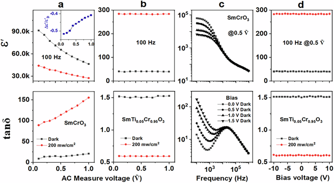
a SmCrO3 sample with AC measure voltage at 100 Hz. b SmTi0.05Cr0.95O3 sample with AC measure voltage at 100 Hz. c SmCrO3 sample with frequency and DC bias voltage. d SmTi0.05Cr0.95O3 sample with DC bias voltage at 100 Hz.
The pristine SmCrO3 sample can be subjected to a DC bias voltage of no more than 2.0 V in the dark, as shown in Fig. 4c. At a measured voltage of 0.5 Ṽ, as the bias voltage increases, the dielectric constant at frequencies below the WG relaxation peak significantly decreases and the loss tangent significantly increases. At frequencies higher than the relaxation peak, the dielectric constant and loss tangent do not vary with bias voltage. If light is added, a bias voltage of 0.2 V can put the LCR instrument in an abnormal working state, just like a bias voltage of 2.0 V or above in the dark (excessive leakage current). For Ti-doped samples (only SmTi0.05Cr0.95O3 and at 100 Hz here), regardless of whether in the dark or under illumination, with a DC bias of −10.0 to +10.0 V, the dielectric constant and loss remain almost unchanged, showing a certain level of voltage resistance, as shown in Fig. 4d.
The SmCrO3 sample and the Ti-doped SmCrO3 sample exhibit significantly different scanning electron microscopy (SEM) morphology. As shown in Fig. 5a, the perovskite SmCrO3 grains exhibit obvious oriented growth and distinct exposed crystal surfaces, with a size of 4–6 μm, and clear grain boundaries. However, all Ti-doped samples are densely packed with 3–5 μm pores. The SmTi0.05Cr0.95O3 sample exhibits 2–3 μm spherical grains with tightly bonded grain boundaries. For the SmTi0.1Cr0.9O3 sample, the number of voids increases, most spherical grains become larger and square, and grain boundaries become more compact. In the SmTi0.2Cr0.8O3 sample, the voids merge and become larger, the grains become larger, and the grain boundaries become tighter. The polycrystalline SmCrO3 sample has numerous grain boundaries, but the resistivity still falls within the semiconductor range, indicating that most of these clear and uniform grain boundaries are conductive. Atoms at grain boundaries deviate from their equilibrium positions and have higher kinetic energy. In addition, there are many defects at grain boundaries, such as holes, impurity atoms, and dislocations. Therefore, the diffusion rate of atoms at grain boundaries is much faster than inside the crystal32,33,34,35,36,37.
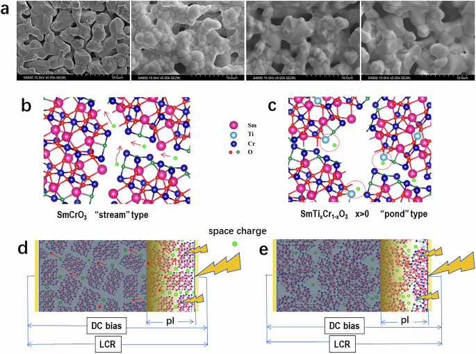
a From left to right are the morphologies of samples with x values of 0, 0.05, 0.1, and 0.2, and the statistical porosity is about 18%, 22%, 25%, and 27%, respectively. b The open space and dangling bonds at grain boundaries promote ion migration, and the charge carriers captured at grain boundaries can also migrate under the action of an electric field, referred to as the “stream” type. c Due to the barrier of the grain boundary, the carriers trapped by the vacancy grain boundary can only form space charges and local states, and cannot migrate under the action of the electric field, called the “pond” type. d Illumination diagram of “stream” type sample. e Illumination diagram of “pond” type sample.
After a small amount of Ti doping, the sample becomes an insulator, indicating that the dense grain boundaries after doping are the barrier layer and non-conductive. The reason for the formation of dense grain boundaries may be that Ti3+ ions near the grain boundaries can interact with oxygen ions in adjacent grains to form Ti4+ ions. The binding energy of Ti ions in the XPS graph (Supplementary Fig. S5) is slightly higher than that of Ti3+, which precisely indicates this point. The Ti4+ ion has a smaller radius, and at the same time, Ti4+ oxide is more insulating, so this dense grain boundary is electrically insulating. In this way, we constructed two model graphs before and after doping. One is the grain boundary conductive model in Fig. 5b, which we refer to as the “stream” type. The other is the grain boundary insulation model in Fig. 5c, We call it the “pond” type.
Here, all SmTixCr1−xO3 (x = 0, 0.05, 0.1, 0.2) samples are opaque, and the depth of light action is only a small part of the thickness of the 1.0 mm sample, as shown at the right end of Fig. 5d, e, respectively. Although the thickness of light action is limited, a large number of electrons excited by light reach the “stream” and flow along the “stream” under the action of an alternating electric field. At lower frequencies, these electrons can flow for a long distance, causing a large amount of space charges such as holes at grain boundaries to annihilate under the action of these photoelectron flows32,35. This may be the reason why the dielectric constant of the SmCrO3 sample decreases and the loss increases at low frequencies when exposed to light. As the frequency increases, the distance of the photoelectron flow becomes shorter, the annihilated space charge decreases, the dielectric constant relatively increases and the loss remains relatively high. Under the action of DC bias, space charges near the boundary “stream” may also form a current. At low frequencies, the larger the bias voltage, the greater the loss current, which is why the low-frequency dielectric constant decreases and the loss increases.
The MW peak of tanδ observed in the dark state shifts to higher frequencies under illumination as shown in Fig. 2a. In the Maxwell–Wagner effect, the peak frequency of tanδ, fpeak, is given38 by
Here, Re and Ce, respectively, denote resistance and capacitance in the regions where photo-excited carriers exist. Rb and Cb, respectively, denote resistance and capacitance in the barrier layers caused by factors such as grain boundaries and sample-electrode interfaces19,38. The number of conductive carriers increases under illumination, and the increment of carriers decreases the resistance Re (Supplementary Fig. S8). This causes fpeak to shift to higher frequencies according to the formula above.
When the SmTixCr1−xO3 sample is illuminated, the photoelectrons may reach the boundary “bond” and combine with other atoms to form new space charges, and the holes will also form space charges. Due to the obstruction of the insulating grain boundary layer, these charges cannot form an electric current under the action of an electric field. That’s why under illumination, the dielectric constant increases several times while the loss tangent remains low. Similarly, the dielectric constant and loss are not related to larger DC biases. After Ti doping, the grain boundaries become insulating, by using the conditions Rb ≫ Re and Eq. 1. The decrease in Re under illumination (Supplementary Fig. S9) is the cause of the shift of the Debye peak towards higher frequencies or the generation of the Debye peak under illumination, as shown in Fig. 2b, c, respectively. Shown in Supplementary Fig. S10, the Nyquist plots of the two samples measured at room temperature. After illumination, the proportion of semi-circular arcs increases, indicating the dominant role of grain boundaries in the optical dielectric properties. From Supplementary Fig. S11, the SmCrO3 sample has relatively low-quality factor values and the overall quality factor values of the SmTi0.05Cr0.95O3 sample are very high. Under illumination, a minimum value appears at 2 kHz, which is the position of the Debye peak modulated by light.
Comparing the PDE in this work with the reported results of other materials (Table 1), it was found that SmCrO3 has unique visible light dielectric properties, as well as ultrasensitive low-frequency visible light PDE of modified SmCrO3, accompanied by excellent insulation performance and low loss, making it a promising candidate for optical dielectric applications. Meanwhile, our work indicates that SmCrO3 provides a new system for studying photo dielectric physics.
Conclusions
Dense and homogeneous SmTixCr1−xO3 was prepared by solid-state sintering. The rate of change of the dielectric constant of the material was negative and then positive with frequency, with a minimum of −51% at 100 Hz (measured voltage 0.1 V) and a maximum peak of +654% around 8 kHz. Although the titanium-doped SmCrO3 sample becomes an insulator, visible light can still modulate the appearance of the Debye relaxation peak and an ultrasensitive low-frequency optical permittivity change of up to +790% is observed in the SmTi0.05Cr0.95O3 sample. Compared with other studies in the field of photodielectricity, it is shown that SmCrO3 material has unique visible light dielectric properties and is an ideal photo-controlled dielectric material. These interesting observations provide further insights into the potential applications of optically controlled devices.
Methods
Sample fabrication
The samples of SmTixCr1−xO3 (x = 0, 0.05, 0.1, 0.2) were compounded by conventional solid-state reaction. The stoichiometric amounts of Cr2O3, Sm2O3, and TiO2 powders with high purity (≥99.99%) were mixed and grounded in an agate mortar and sintered at 1400 °C in the air for 1000 min, repeated three times. Then the disk samples about 8 mm in diameter and slightly thicker than 1.0 mm in thickness were pressed under 40 MPa pressure and sintered at 1450 °C in air for another 1000 min and cooled down to room temperature with three degrees per minute.
Sample characterization
The samples were characterized by XRD at room temperature using PANalytical Empyrean. Surface morphologies of the samples were detected by SEM (model: S-4800). XPS analysis was performed using a Thermo Scientific K-Alpha electron spectrometer from Thermo Scientific Corporation.
Sample measurement
Magnetization data were collected with a Physical Property Measurement System (Quantum Design) With an applied external magnetic field (H) of 100 Oe, the M–T curves in zero field cooling mode were measured over the temperature range of 5–300 K. The current–voltage (I–V) characteristics were measured with a Current and Voltage Source Meter (Keithley 2400) by applying a pulse DC voltage across the pellets with an interval of 5 s between the two sequent pulses. The temperature, frequency, and bias voltage-dependent dielectric properties (capacitance and loss tangent) were tested by a precision impedance analyzer 6500B (Waynekerr Corp.) in the frequency range of 20 Hz–1000 kHz at different temperatures in a range of 77–400 K.
Samples for dielectric measurements were polished to a thickness of 1.0 mm, and about 40 nm thick Au electrodes were deposited on both sides of the pellet by magnetron sputtering through a metal mask in order to enable the visible light to act on the sample. The incident light was irradiated from one side of the electrode. The transmittance of the Au electrode is about 30%. The irradiation intensity used in this work was the outlet value of the light source. an ordinary low-voltage halogen lamp (12 V, 100 W) with a wavelength of about 400–780 nm was used as the light source, in which the intensity at the light source outlet is adjustable, with a maximum intensity of 200 mW/cm2. Monochromatic light at 405, 785, and 905 nm is generated by light-emitting diodes, and the maximum light intensity of the outlet is also 200 mW/cm2. All light irradiation experiments were conducted at room temperature.


Responses