Ultraviolet irradiation penetration depth on TiO2
Introduction
Metal oxides (MOs), e.g., TiO2, are widely used for solar energy, battery, sensor, and biomedical applications1,2,3,4,5,6,7. The ability to tune their properties (e.g., electrical, chemical) without altering desired characteristics and their relatively low cost are major reasons for their widespread use8,9,10,11. To this end, it is known that the ultraviolet (UV) irradiation of MOs plays an important role in many applications12,13,14. More specifically, high-energy UV (a.k.a., UVC) irradiation can change surface stoichiometry and chemistry by introducing photoinduced surface oxygen vacancies (PI-SOVs) and through resulting chemical reactions (e.g., formaldehyde formation of methanol on Ti5c sites)10,15,16,17,18.
TiO2, a wide bandgap semiconductor (Ebg > ~3 eV), absorbs light (λ < ~400 nm)11,19,20. However, PI-SOVs are sensitive to irradiation wavelength and are induced only by UVC irradiation (λ < 280 nm)10,15,16,21. Although the existence of PI-SOVs is well-supported, there is no agreement on the penetration depth of the UVC22,23,24,25,26,27,28,29. Being the nucleus of a decades-old interest, the claims of the penetration depth of UVC range between 10-30 nm up to the micrometer level22,23,24,25,26,27,28,29. The uncertainty of the UVC penetration depth not only hinders the complete understanding of UVC-sample interaction but also impedes the longevity of sample systems where TiO2 is used as an electron transfer and/or UV protection layer30. Formerly, Raman spectroscopy and time-resolved atomic force microscopy (TR-AFM) were utilized to explore the effect of PI-SOVs10,15,16,17,31. In our previous works, we performed TR-AFM measurements to understand the influence of UVC irradiation and/or photocatalytic reactions on the charge carrier dynamics of TiO2 and similar sample systems15,17,31.
Here, we measured the transmission and the effect of back illumination of UVC (λ = 255 nm) irradiation on a polycrystalline TiO2 film and a single-crystal TiO2 sample. Our measurements show two major findings, which are important for the basic understanding of UVC-MO interaction and potentially, for MO-based device design. First, even though the majority of incident UVC is absorbed within the first few tens of nanometers, the UVC irradiation has a measurable transmission even through 500 μm-thick samples. Moreover, as expected, the measured transmission is inversely proportional to the TiO2 thickness and the illumination density. Second, the effect of back illumination of UVC has a dominant influence on the charge carrier dynamics, which has been quantified via TR-AFM measurements as a function of UVC illumination density for the single crystal TiO2 sample. We believe that the observed variation of charge carrier dynamics and its dependence on back illumination power density originates from the PI-SOVs and their collective motion. Our results reveal that the effect of UVC irradiation on MOs can extend through hundreds of micrometers and alter carrier dynamics in TiO2 across the bulk. We believe our results are important for a fundamental understanding of the interaction of UVC with MOs and for the design of sample systems utilizing MOs in which TiO2 is employed either as an electron transfer or UV protection layer.
Results and Discussion
We performed measurements to reveal the penetration depth of UVC irradiation and its effect on charge carrier dynamics. First, we performed optical transmission measurements via back illumination (vide infra) on a fused silica glass substrate, polycrystalline TiO2 film, and 500 μm-thick, undoped TiO2 (100) single crystal. The optical transmission measurements of fused silica reveal ~90% of UVC transmission, as classified by the manufacturer. Figure 1 summarizes that the optical transmission is inversely proportional to the luminance of the UVC source, i.e., with increasing illuminance, the UVC transmission of both polycrystalline TiO2 film, and 500 μm-thick, undoped TiO2 (100) single crystal decreases asymptotically. We believe that this inverse relation with illuminance is associated with the PI-SOV density. It is well-known that UVC irradiation results in oxygen vacancies on the surface (vide supra)10,15,16,21. With increasing PI-SOV and electron/hole concentration, mid-gap states are introduced, and as our experiments show, the absorption of UVC irradiation increases32,33,34. Normally, defect engineering is performed in TiO2 to enhance the optical absorption in the visible spectrum for enhanced photocatalytic performance35,36,37,38,39. However, our measurements demonstrate that the optical absorption of TiO2 increases (i.e., optical transmission decreases) even for UVC irradiation. We also experimentally measured the relation between the film thickness and the optical transmission. Although the 46 nm-thick TiO2 film absorbs almost 99% of UVC irradiation, the 500 μm-thick TiO2 (100) single crystal has a measurable UVC transmission across the sample (0.6 – 1% depending on the illuminance). For this reason, our optical transmission measurements show that even though a major part of UVC irradiation (~ 99%) is absorbed within the first tens of nanometers, the rest can penetrate through the entire crystal for hundreds of micrometers. Even though the optical transmission decreases with increasing illumination density monotonically, at very low illumination density levels, i.e., closer to zero, the error propagation is dominated by the operation principle of the UVC diode, as the power consumption, so the illumination of the diode oscillates for voltages closer to the threshold voltage of the diode.
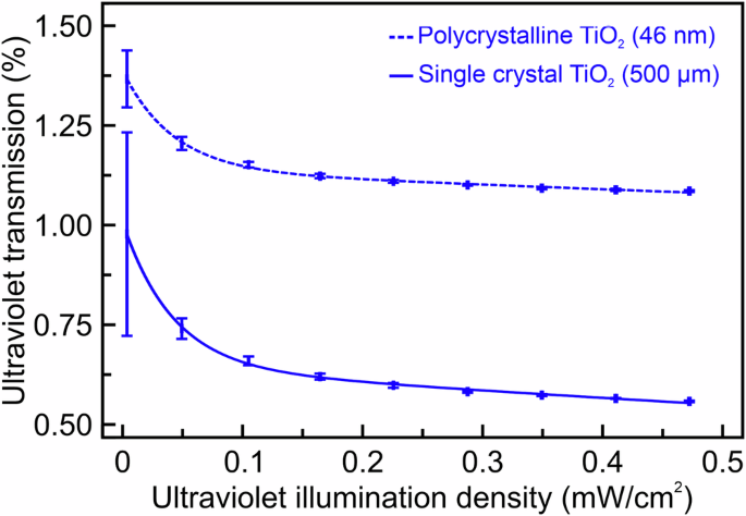
Our measurements on 46nm-thick TiO2 polycrystalline film show that ~99% of UVC irradiation was absorbed within the first tens of nanometers. However, the optical transmission measurements of the 500 μm-thick TiO2 (100) single crystal show that the rest of the UVC (~1%) can penetrate through the entire crystal for hundreds of micrometers. Our measurements for both 46nm-thick and 500 μm-thick samples display that with increasing UVC illumination power density, the optical transmission decreases, i.e., absorption increases. We believe that the enhanced absorption is associated with mid-gap states introduced by the photoinduced oxygen vacancies generated by UVC irradiation.
We also performed TR-AFM measurements on a TiO2 single crystal and a 46 nm-thick polycrystalline film as a function of the back illumination density of UVC irradiation, as shown in Fig. 2. Surface oxygen vacancies in TiO2 (Vo) can have multiple different charge states, where they can be neutral (i.e., Vo0) or charged (e.g., Vo+ and Vo2+)40,41. Former theoretical work showed that the Vo+ state is the thermodynamically most favorable state and has the greatest influence on the TiO2 sample conductivity15,41,42. Thus, we expect to mainly induce the Vo+ vacancies and measure their effect on the charge carrier migration dynamics18.
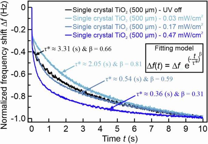
Charge carrier dynamics were accessed by fitting a stretched exponential function to the resonance frequency shift, Δf, as a function of time, t, (Delta fleft(tright)=Delta ftimes {exp }^{-{(t/{{{rm{tau }}}}^{* })}^{{{rm{beta }}}}}). The time constant, τ*, is associated with the decay of the electrostatic interaction within the probing volume and is linked to the charge carrier migration. The stretching factor of the exponential fit, β, is related to the collective motion of charge carriers. We normalized the resonance frequency shifts to enable the comparison of decays for different back illumination levels. Data show that with increasing back illumination irradiation density, measured τ* values decrease monotonically. The decrease of τ* implies an attenuation of charge carrier migration velocity and mobility, which can be associated with enhanced vacancy concentration. The variation of β implies that charge carriers interact more collectively at high irradiation levels. Data presented in this figure were recorded on the same sample region, i.e., the only change between different data points is the UVC illumination densities.
Our TR-AFM measurements on TiO2 single crystal show that the time constant associated with charge carrier migration, τ*, decreases with the existence of UVC illumination. The charge transfer of MOs is mainly governed by holes, electrons, and ions7,18,43,44. For TiO2 samples, in addition to a supplemental ion influence, mainly, electrons and holes govern the sample conductivity7,18,24,45,46,47. Based on the timescale of the measurement (from hundreds of milliseconds to a few seconds), it is expected that we are measuring the migration of slow charge carriers in the sample, i.e., holes as part of small polarons14,18,31,48,49. More specifically, for a single point measurement, τ* values decrease from 3.31 ± 0.87 seconds to 2.05 ± 0.19 seconds even for the lowest illuminance density of 0.03 mW/cm2. In addition, with increasing UVC illuminance, however, τ* decreases almost an order of magnitude compared to UVC off case, i.e., decreases to 0.36 ± 0.08 seconds from 3.31 ± 0.87 seconds for UVC illumination density of 0.47 mW/cm2. It is known that the mobility and velocity of charge carriers are linearly correlated to the measured time constant31. For this reason, the decrease in the τ* implies a decrease in the mobility of charge carriers. Moreover, we observed a prominent decrease in β values with increasing UVC illuminance, i.e., β decrease from 0.66 ± 0.05 (no UVC illumination) to 0.31 ± 0.06 (UVC illumination density of 0.47 mW/cm2). The decrease in β values implies that the charge carriers move more collectively with increasing PI-SOV density. Hence, we believe that the enhanced collective motion can be explained by the increased density of charge traps formed by PI-SOVs50,51,52,53. Nevertheless, as Fig. 1 shows, ~99% of incident UVC were observed within the first few tens of nanometers, i.e., only ~0.6% of the incident UVC reaches the front side of the 500 μm-thick sample. For this reason, it may be claimed that the transmitted UVC may be responsible for the observed variation of τ*and β by introducing PI-SOVs on the front side. Even though the transmitted UVC, i.e.,~0.6% of the back illumination density (~2.4 μW/cm2) may be capable of promoting PI-SOVs on the front side of the sample, the former study has shown that the variation of τ* is linearly correlated with the illumination density and even for significantly higher front illumination densities, the variation of τ* was significantly lower17. For this reason, in this study, the strong variation of τ* (i.e., 10-fold variation) implies that the remaining UVC density is, potentially, not responsible for the observed change. Also, for the back-illuminated sample, the value of β, a parameter for collective motion, decreases by 50%. However, for front-illuminated samples, the variation of β is inert to UVC irradiation. Hence, driven by the concentration variations, we propose that PI-SOVs at the back side of the sample may migrate across the bulk. Nevertheless, back-surface-illuminated X-ray photoelectron spectroscopy measurements or atomic resolution scanning probe microscopy measurements under ambient conditions are required to directly quantify the diffusion of PI-SOVs. However, such measurements are beyond the scope of this work. To distinguish the contribution of PI-SOVs and holes as part of small polarons, we performed complementary back illumination measurements with a low-energy UV (UVA) irradiation (λ = 375 nm), which only introduces electrons and holes but not PI-SOVs10,15,16,21. Our optical transmission measurements for UVA show that, similar to the UVC case, UVA transmission decreases with increasing illumination density asymptotically. However, UVA measurements revealed that the τ* decreases only 50% upon back illumination of the single crystal TiO2 sample, and the corresponding β change is only 10%. To this end, the comparison of UVA and UVC measurements also implies that PI-SOVs dominate the dynamic properties of holes as part of small polarons.
We challenged the reproducibility of our TR-AFM results on a single-crystal TiO2 sample by performing measurements over a span of two weeks under different UVC illumination levels, as Table 1 summarizes. To this end, we conducted successive measurements on ten different sample regions. We performed measurements at a minimum of 25 different points at each region and repeated measurements 40 times at each point, i.e., a total of a thousand measurements for each region. Our repetitive experiments on different sample regions and/or under different illumination levels undoubtedly showed that the observed variation originates from high-energy UVC irradiation.
Our measurements on 46 nm-thick polycrystalline film show that the τ* values are significantly smaller compared to the single crystal sample regardless of the UVC irradiation, as shown in Fig. 3. Former TR-AFM measurements on similar TiO2 films also disclosed smaller time constants compared to single crystals15. We measured the average grain size of our polycrystalline film as 8.7 ± 4.0 nm. The significantly smaller time constants may be associated with the grain size, orientation, and the (degree of) polycrystallinity of the films54,55,56,57,58,59,60. The grain size and orientation may affect the formation of PI-SOVs and electron/hole pairs, altering the charge carrier migration dynamics56,57,60. However, the identification of the intrinsic contribution of such effects is beyond the scope of this work.
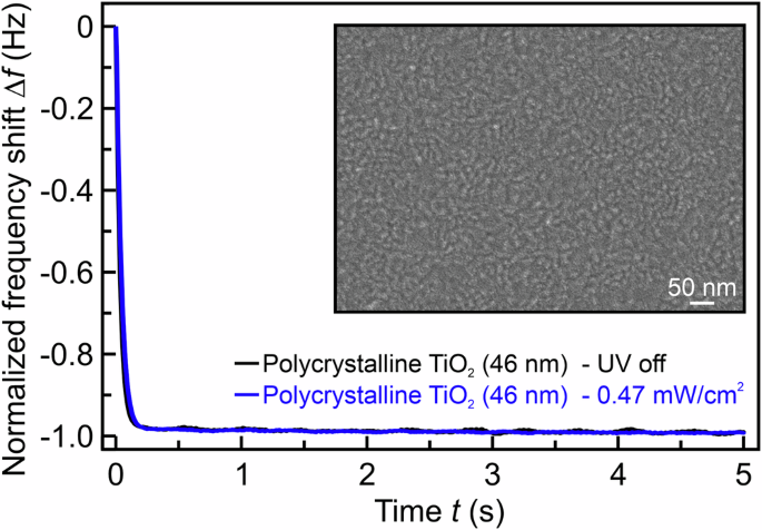
Our measurements show that the time constant associated with the charge carrier migration is significantly smaller than the single crystal TiO2, regardless of the existence of UVC irradiation. As the measured time constant is very close to the detection limit, we do not deliver a numerical value. As shown in the inset, we performed scanning electron microscopy measurements, which revealed that the average grain size has an equivalent circular diameter of 8.7 ± 4.0 nm. We believe that the smaller time constant is related to the grain size, orientation, and degree of polycrystallinity of the film (see main text for details).
Even though oxygen vacancy formation due to UVC irradiation is expected to be a surface phenomenon, as ~99% of incident UVC is absorbed within the first tens of nanometers, our TR-AFM measurements show that the effect of UVC irradiation can penetrate deep into the bulk and can alter electronic properties for hundreds of micrometers across the sample. This result is important not only for the basic understanding of the variation of charge carrier dynamics due to PI-SOVs in MOs but also for sample systems that employ MOs as a charge transfer layer or protecting layer for underlying photocatalytic activities.
Conclusions
We performed optical transmission and time-resolved atomic force microscopy (TR-AFM) measurements on back-illuminated (with high-energy ultraviolet (UVC) irradiation, λ = 255 nm) metal oxide (MO) samples, i.e., a 500 μm-thick, undoped TiO2 (100) single crystal and a 46 nm-thick polycrystalline TiO2 film grown on fused silica glass. Our optical transmission measurements show that even though ~99% of incident UVC was absorbed within the first tens of nanometers, the residual illuminance (i.e., ~1%) can penetrate through the bulk for hundreds of micrometers. Moreover, we revealed that the optical transmission is inversely correlated with the illumination density. We think that this inverse relation between the optical transmission and the illumination density arises from the enhanced concentration of mid-band gap states prompted by photoinduced surface oxygen vacancies. Our TR-AFM measurements show that the time constant associated with the charge carrier migration is strongly affected by the back illumination density and can decrease almost by an order of magnitude with increasing UVC irradiation density. Moreover, the collective nature of charge carrier migration is more pronounced with increasing irradiation density. Also, the charge carrier migration dynamics and its control are important for other oxides such as SrTiO3 and KTaO361,62,63. It is important to note that atomic scale identification of oxide-based devices and correlating the measured dynamic characteristics at the interface of different material systems as a function of their intrinsic properties (e.g., bandgap, intrinsic and extrinsic doping, roughness), external stimulation (e.g., temperature variation, chemicals), and transient formation/recovery of PI-SOVs remain to be explored. For this reason, we believe our results will lay the foundation for a more fundamental understanding of UVC penetration and MO-based sample systems.
Methods
Sample preparation
Preparation of polycrystalline TiO2 films
46 nm-thick polycrystalline TiO2 film was prepared on a fused silica glass substrate using molecular beam epitaxy (MBE)64,65. The silica glass (by MTI Corporation, UV Grade Fused Silica Glass) was cleaned at 500 °C in a 2.0 × 10⁻⁶ Torr O2 atmosphere for 60 mins in the ultra-high vacuum chamber before the growth. The TiO2 film was later prepared in the same MBE chamber. The substrate temperature was at 500 °C during the growth. The Ti flux of ~1.1 × 10¹³ atoms·cm-2·s-1 (measured using quartz crystal microbalance) was employed. The O2 partial pressure was 2.0 × 10⁻⁶ Torr during the growth. The film thickness was confirmed by fitting X-ray diffraction reflectivity measurements.
Preparation of TiO2 (100) single crystal
We utilized a 500 μm-thick, undoped TiO2 single crystal (by MSE Supplies LLC). We followed an established recipe, as detailed elsewhere15,17,31,42,66. Briefly, TiO2 crystal was annealed at 1000 °C for 10 hours, in addition to heating and cooling periods (~3 hours each). This method creates rutile-terminated, atomically flat terraces that are free of carbon clusters (please see Section 1 of the Supplementary Information for further details)15. Avoiding large clusters of contamination is important both for the stability of the TR-AFM measurements and to able to extract intrinsic properties of MBE-grown thin films (vide supra) and single crystals.
We used a rutile-terminated surface, as the anatase termination is more susceptible to particles in the air under UVC irradiation and ambient conditions67,68,69,70,71. For this reason, adsorbed, undesired particles could impede the characterization of charge carrier dynamics and their variation with PI-SOVs.
Being a slightly more stable configuration compared to the (100) surface, in TiO2 (110), Ti atoms can have either five or six coordination numbers, while the coordination number of the (100) surface is constant and five72,73,74. Our focus in this work is to understand the penetration depth of the UVC irradiation and its electronic effects across the sample, rather than revealing site-dependent variation of charge carrier dynamics. For these reasons, to eliminate any coordination number-dependent variation of time-resolved properties, we employed a TiO2 (100) surface as our single crystal sample.
Back illumination of samples with ultraviolet illumination
We used a constant wavelength (λ = 255 nm), UVC light-emitting diode (LED, OP255-10P-SM by Crystal IS). As Fig. 4 shows, the UVC source was shielded to ensure that the surface was only back illuminated via the cavity underneath the sample. The power density of the transmitted light was measured with a power meter (Slim Photodiode Power Sensor, S130VC by Thorlabs). The measurement setup was optically isolated to ensure no external light affected the measurement. We tuned the power of the UVC source to understand the effect of illumination density. The distance between the power meter and the sample was kept constant for each measurement. The back illumination of the sample is uniform and covers the entire back side of the sample, as the illumination angle of the UVC diode is 120°, and the optical cavity is ~1 cm away and right above the UVC diode.
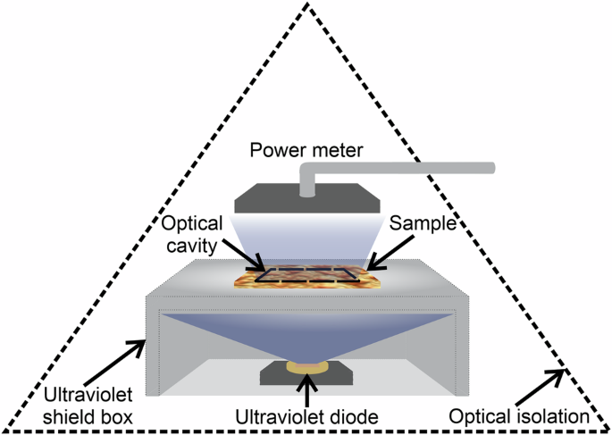
A UVC diode (λ = 255 nm) was employed to back illuminate samples as a function of metal oxide (MO) thickness and illumination density. The UVC transmission was measured with a power meter. The UVC diode was shielded within a metal box with an optical cavity under the sample, eliminating any UVC leak to the optical power meter. Additionally, the entire measurement setup was optically isolated to prevent any external influence on measurements.
We positioned the UVC diode on a large stainless steel heatsink with an embedded thermocouple (PT-1000 with a temperature resolution of 0.01 °C) right under. The maximum power dissipation of the diode is 0.8 Watts, and we did not observe any meaningful temperature variation due to the operation of the LED. Moreover, the temperature in the laboratory was 19.6 ± 0.4 °C, while the corresponding relative humidity level was 38 ± 3% with active temperature and humidity controls to avoid confounding contributions on samples and measured quantities. Finally, as the concentration of PI-SOVs stabilizes within ~90 minutes, we waited for the stabilization of the formation and recovery of PI-SOVs for our measurements15,16.
Time-Resolved Atomic Force Microscopy Measurements
Integrated with new hardware and software, we employed a customized VEECO EnviroScope system for our TR-AFM measurements. Details of microscope customization and principles of TR-AFM measurements can be found elsewhere75. Briefly, as summarized in Fig. 5, a voltage pulse, Vbias, was applied between the sample and the oscillating cantilever probe after the tip was retracted away (e.g., 15 nm) from the surface. The applied Vbias results in a time-dependent Coulombic interaction, which causes the migration of charge carriers. The migration of charge carriers leads to a time-dependent tip-sample interaction force, which induces the time-dependent resonance frequency shift of the cantilever probe, Δf. For conventional TR-AFM measurements, the Δf is demodulated with a phase-locked loop and the stretched exponential function is fitted to the time, t, versus Δf data76,77,78,79. The time constant associated with the Δf decay, τ*, corresponds to the charge carrier dynamics of ions, holes, or vacancies depending on the sample system76,77,78,79,80,81,82. This measurement principle was formerly employed for Li+ transport in LiAlSiO4, K+ transport in K2O.2CaO.4SiO2 glass, and Na+ transport in Na2O.GeO2 glass, hole migration in TiO2, and oxygen vacancy migration in SrTiO315,17,31,42,76,77,78,79,83. The stretched exponential term, β, can have a value between zero and one while representing the collective motion of charge carriers80,81,82. Specifically, decreasing β values imply enhanced collective motion, i.e., stronger particle-to-particle interaction.
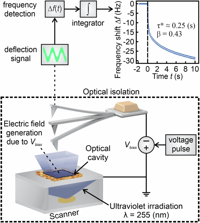
A voltage pulse, Vbias (e.g., a voltage step with an amplitude of 5 V), was applied between the tip and the sample, which resulted in a time-dependent Coulombic interaction. The variation in the induced electric field introduces a time-dependent tip-sample interaction force, which leads to the resonance frequency shift of the oscillating cantilever probe, Δf (demodulated with a phase-locked loop). The experiment was repeated on the same lateral position to enhance the signal-to-noise ratio. A stretched exponential fit was applied to the Δf as a function of time, t, as presented with a dashed line. The decay of the stretched exponential fit, τ*, is related to the migration dynamics of charge carriers (see main text). The stretching factor, β, is associated with the collective motion of charge carriers (see main text). A UVC source (λ = 255 nm) was employed to back illuminate samples with different illumination densities to explore the effect of back illumination on charge carrier dynamics. The microscope chamber was optically isolated from the outside to eliminate any external UVC contributions. The UVC source was also isolated in a metal box to ensure the back illumination of samples via an optical cavity that was at least 50% smaller than the sample area. The data presented in this figure were recorded at room temperature on a TiO2 (100) single crystal with a back illumination density of 0.47 mW/cm2.
We repeated measurements at least 25 different sample locations and at each position 40 times to ensure that the back illumination of the surface covers the entire sample and to enhance the signal-to-noise ratio42,83. For all of our measurements, we implemented a gold-coated, conductive microcantilever (OPUSTIPS, 4XC-GG, tip radius < 30 nm, stiffness −9.0 N/m, and resonance frequency −150 kHz). To secure the back illumination, the sample was attached to a shielding box with an opening underneath and positioned directly on the UVC source (vide supra). The microscope chamber was also isolated optically. Finally, it was previously shown that the UVC illumination does not change the sensitivity or the temperature of the oscillating cantilever31.
Responses