Understanding the deformability of 2D van der Waals materials from the perspective of chemical bonds

Introduction
Embracing a wide range of chemical compositions from single-element graphene, to binary transition metal dichalcogenides (TMDCs), and ternary or multi-nary materials, two-dimensional (2D) van der Waals (vdW) materials exhibit rich physical properties and find promising applications in electronics1, catalysis2, biology3, and energy utilization4, etc. The fascinating diversity in both compositions and the physical properties comes essentially from the combination of strong intralayer bonds and weak interlayer vdW interactions5. The intralayer bonds constitute the framework of the materials, fundamentally deciding the lattice rigidity, electronic band structure, and phonon dispersion. They also act as the main channel for the transport of particles or quasi-particles, e.g., electrons and phonons. The interlayer vdW interactions, although much weaker than the intralayer bonds, act sophisticatedly in modulating various exotic properties6,7.
In addition to the widely studied physical properties, mechanical properties are also important to 2D vdW materials8, especially in the face of the rapidly developing intelligent era. On the one hand, flexibility (or simply elastic bending deformability) is essential for mono- or few-layer materials to adapt to non-flat and wearable devices9,10. On the other hand, when multiple layers are stacked together, the interlayer interactions become noticeable and even govern some mechanical behaviors11,12,13. Different from the elastic bending of the monolayer, the deformation of the multi-layer or bulk crystals often involves irreversible processes, a kind of plastic deformation. The plasticity is different from the low-dimension-induced flexibility, but a more intrinsic mechanical property for bulk materials, which allows the material to be readily processed into various shapes like metals with low lost12. In this case, the interlayer slip/glide is the most common mechanism for deformation, which is also key to a series of important physical effects such as super lubrication14,15, interfacial ferroelectricity16,17, and phase transition18. Interestingly, exceptional plasticity has been recently discovered in a series of 2D vdW bulk crystals like InSe19,20,21,22 and SnSe223, adding a new facet to these materials and offering new possibilities for efficient fabrication and diversified application24,25,26.
In view of the remarkable plasticity in these 2D vdW materials, it rises as an important and interesting topic to understand the deformation mechanism. As commonly conceived, the interlayer slip is certainly the dominant process, but such a mechanism cannot solely rationalize the large plasticity, especially the compressibility along the vdW gap. To this end, several indispensable mechanisms have been proposed for this large plasticity, such as the cross-layer dislocation slip19,27, local structural transition28,29, and layer buckling30. However, a general principle regarding deformability seems still missing beyond specific material systems.
From the perspective of chemical bonding, although there can be complicated mechanisms involving the microstructures and defects, the intralayer and interlayer interactions should be the basic aspects in analyzing deformability for these 2D vdW materials. Previous studies have outlined the trend of crystal orbital Hamilton population (COHP)31 during the slip process for specific typical materials20,27,32,33,34. However, the general correlations between chemical bonds and mechanical properties are to be explored for a variety of materials, which is key to comparatively understanding and developing deformable vdW crystals.
In this work, focusing on typical hexagonal 2D vdW crystals, we probe the correlations between atomistic bonding features and mechanical properties by using the DFT calculations. Both intralayer and interlayer bond strength are quantified by the integrated crystal orbital Hamilton population (-ICOHP). The cleavage energy, slip barrier energy, and modulus are found to be strongly correlated with -ICOHP, even in a linear way in some cases. The IIIA-VIA compounds (GaS, GaSe, InSe) are predicted to show better deformability than graphite, BN, and MoS2, as reflected by the larger deformability factor. It is also anticipated that the deformation behaviors can be well-modulated by constructing superlattices. These findings offer a fundamental yet generalized insight into the vdW materials’ deformability.
Methods
Structure relaxation and bond analysis
First-principles calculations were carried out using the projected augmented wave (PAW) method35 as implemented in the Vienna Ab Initio Simulation Package (VASP)36,37. After testing different functionals (see Fig. S1), the Perdew-Burke-Ernzerhof (PBE)38 generalized gradient approximation (GGA) was finally used for the exchange-correlation terms, and DFT-D3 method was used to correct the van der Waals interactions39. A 500 eV cut-off energy for plane waves was adopted. The energy convergence criterion and force convergence criterion were 10−5 eV and 0.01 eV Å−1, respectively. The k-point mesh generated by Γ-centered scheme with a resolution better than 0.04π Å−1 was used for primitive cell relaxation40. The lattice constants were well described compared to experimental data (see Table S1). The COHP analysis was carried out by the local orbital basis suite toward the electronic-structure reconstruction package (LOBSTER)41. The basis set for COHP analysis is pbeVaspFit2015 and the charge spilling is smaller than 2%.
Cleavage energy and generalized stacking fault energy (GSFE)
Slab models with a 20 Å vacuum region were prepared for cleavage energies and slip energy barriers calculations. The cleavage energy can be calculated by the following expression42:
where ({E}_{{slab}}-{E}_{{bulk}}) is the energy difference between the slab model and bulk material, (A) is the cleavage surface area. The slip energy can also be calculated with a similar method, replacing the numerator with the energy difference between the slipped structure and initial structure27. For interlayer slip, slabs with no less than 12 layers were constructed. In order to obtain GSFE mapping of interlayer slip, 100 intermediate steps (divide one crystallographic period into 10 steps along the a and b directions) were considered and the equivalent structures were only calculated once. The points along the slip path were double-sampled to get accurate interlayer slip energy barriers. As for cross-layer slip, slabs with slip plane (1(bar{1})0) ((110) plane for graphite) exposed to vacuum were constructed, and each slab contained over 48 atoms. Cross-layer slip was divided into 20 steps, and the GSFE of each step was calculated to search the slip energy barriers.
Elastic properties
The elastic moduli were calculated using the energy-strain method by VASPKIT code43. For these hexagonal vdW crystals, there are five independent elastic constants (C11, C12, C13, C33 and C44). Due to the transverse isotropy, the in-plane elastic modulus is the same along the x and y directions. The in-plane modulus Exy and out-of-plane modulus Ez can be calculated according to the following formulas44:
Result and discussion
Chemical bond quantification
As shown in Fig. 1a, due to the layered structure, the interlayer interactions and intralayer interactions exhibit quite different characteristics. To describe these interactions, we resort to the crystal orbital Hamilton population method (COHP) (see Fig. 1a). The negative integrated value (-ICOHP) is regarded as the bonding energy caused by orbital overlap. For the interlayer interactions, the precise description has always been a challenge for the vdW materials since the -ICOHP cannot fully embrace the vdW interactions, especially the dispersion interactions31. Despite this, the values of -ICOHP could change when crystal structures are relaxed and corrected by vdW interactions. Here we still tentatively employ the -ICOHP per unit area to estimate the interlayer interactions (see Fig. 1b, where only the bonds crossing the slip/cleavage planes are included.). It is seen that the TMDCs (MoS2, MoSe2, WS2) stand out with the highest values among these vdW crystals. These results are reasonable according to the previous work27,45, which indicates that the interlayer cleavage energies of TMDCs are relatively high. Contrary to the weak interlayer interactions, the intralayer bonds can be described in a more reliable manner. As shown in Fig. 1b, the intralayer bond strength of h-BN and graphite is much higher than the other materials. This is consistent with our common sense that the shorter B-N and C-C bonds are very strong. As for IIIA-VIA compounds, the law between bond length and strength well applies: the intralayer In-Se bonds are among the longest, which leads to the weakest interactions.

a Schematic illustration. b -ICOHP per unit area (A) for interlayer interactions and -ICOHP per cation-anion bond for intralayer bonds.
Slip and cleavage energies
Figure 2 shows the cleavage energies (Ec) and slip energy barriers (Eb) of typical hexagonal-structured vdW crystals. By definition, Ec is the energy required to break bulk materials into two parts; Eb is defined as the maximum slip energy along the easiest slip path that can be deduced from the generalized stacking fault energy (GSFE) (see computation methods for details)46. The interlayer and cross-layer behaviors are schematically depicted in Fig. 2a, d, respectively.
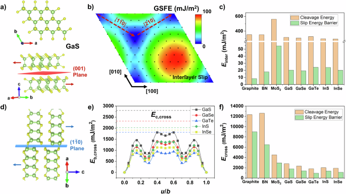
a Crystal structure of GaS; the red plane represents the interlayer slip plane. b GSFE mapping of interlayer slip ((001) plane) for GaS; the black dots represent intermediate steps of slipping, and the red dash arrows depict the slip path with the lowest energy barrier. c Interlayer cleavage energies (orange) and slip energy barriers (green) for typical 2D vdW materials. d Cross-layer slip for GaS; the blue plane represents the slip plane. e GSFE curves of cross-layer slip for IIIA-VIA group compounds; u/b is the ratio of slip distance to the Burgers vector; dash lines represent cross-layer cleavage energies of materials with corresponding colors. f Cross-layer cleavage energies and slip energy barriers for 2D vdW materials.
For the interlayer slip, we sampled the whole GSFE surface with a uniform mesh (black dots on the GSFE surface of Fig. 2b, each dot represents a slip step). Consistent with the structure symmetry, all these materials have a similar interlayer slip profile. The interlayer slip paths with minimum energy barrier are all along the 1/3[1(bar{1})0] +1/3[210] direction (arrows in Fig. 1b and Fig. S2). The Eb,inter of these IIIA-VIA materials (GaS, GaSe, GaTe, InS, InSe) are all around 20 mJ/m2, while their Ec,inter values are close to 300 mJ/m2 (see Table S2). As expected, graphite, which is widely used for lubrication, exhibit even lower Eb,inter of 8.4 mJ/m2. Interestingly, MoS2 has the highest Eb,inter (54.6 mJ/m2) and Ec,inter (562 mJ/m2) among these materials. These values are also consistent with the previous reports27,45,47,48,49,50, which echoes the larger interlayer interactions of MoS2-like TMDCs (Fig. 1b).
The atomistic model of cross-layer slip and calculation results are shown in Fig. 2d–f. Based on the previous study27, the cross-layer slip plane is taken as the (1(bar{1})0) plane (the blue plane as shown in Fig. 2d) for h-BN, MoS2, IIIA-VIA group compounds, and (110) plane for graphite (see Fig. S3 for details). All of the cross-layer slip is set along [001] direction according to previous studies for simplicity27. Compared to interlayer slip (Fig. 2c), the cross-layer slip exhibits tens or even hundreds of times higher energy barriers (Fig. 2f), which well corresponds to the much stronger intralayer bonds. As shown in Fig. 2e, for the IIIA-VIA compounds, although the cross-layer GSFE curve profiles are still similar to each other, the Eb values are vastly different. The highest Eb,cross 1806 mJ/m2 for GaS is almost twice that of GaTe (937 mJ/m2). As shown in Fig. 2f, the IIIA-VIA materials seem to easily to incur cross-layer slip when compared with others, which is also fundamentally determined by the intralayer bond strength, as to be discussed later. Those materials with high Ec,cross usually exhibit high Eb,cross as well.
Correlation between chemical bond features and slip/cleavage energies
Based on the above discussion, the slip/cleavage energies are closely related to the bonding characters. Here in this section, we try to give some correlations between bonding features and mechanical properties. (see Fig. 3 and Fig. S4). Figure 3a, b shows that there is a moderate positive relationship (the Pearson correlation coefficient, r = 0.80 and 0.79) between interlayer cleavage/slip energies and -ICOHP per unit area, while the linearity is not so high (the linearity coefficient, R2 = 0.58 and 0.56). This is reasonable since -ICOHP cannot fully capture the weak and sophisticated interlayer interactions as mentioned above. Even so, MoS2 with the highest interlayer -ICOHP per unit area still exhibit highest Ec,inter and Eb,inter among these materials. As shown in Fig. 3c, d, the cross-layer cleavage/slip energies versus -ICOHP per unit area are found to be more correlated (r = 0.98 and 0.99; R2 = 0.96 and 0.99). Among them, graphite and h-BN show the strongest bonds and, thus, the largest slip/cleavage energies.
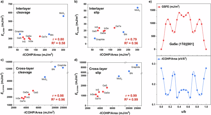
a Interlayer cleavage energies, (b) slip energy barriers versus total -ICOHP per unit area for the interlayer (001) plane. c Cross-layer cleavage energies and (d) slip energy barriers versus total -ICOHP per unit area for the cross-layer (1(bar{1})0) plane ((110) plane for graphite). e GSFE, -ICOHP per unit area for (1(bar{1})0) [001] slip system in GaSe as a case study. The r and R2 represent the Pearson correlation coefficient and the linearity coefficient, respectively.
Figure 3e shows the variation of GSFE (upper panel), and -ICOHP (lower panel) with the displacement for the cross-layer slip of GaSe as a case study. It is notable that GSFE and bond interaction (-ICOHP) have an opposite trend during the slip process. This means that additional energy (increase in GSFE) is needed to break bonds (decrease in -ICOHP). A similar phenomenon could be observed in other hexagonal vdW materials (see Fig. S4). The local minimum of GSFE is at about 0.3 u/b for GaSe, corresponding to new bond formation between adjacent layers. At this stage, the slipped layer of GaSe appears like a claw-catching layer on both sides of the vdW gap (see Fig. S5), so that the interlayer cleavage can be refrained. By contrast, this characteristic is hardly observed in h-BN and graphite vdW crystals with flat layers. This is probably related to the weaker and more ionic (less covalent) Ga-S bonds as compared to C-C and B-N bonds. It is worth mentioning such a successive bond-breaking and reconstruction scenario not only holds for the ideal slip process. Recent studies have found that the localized micro-cracks, the prototype transition, and the martensitic transformation contribute to plastifying InSe crystals28,51. Indeed, all these mechanisms involve the above-mentioned bond-switching process. For vdW crystals, the hierarchic bonding features, the pliable monolayers, and the strong anisotropy will provide a large room for the activation of rich deformation mechanisms.
Elastic property and its bonding origins
Other than cleavage energy and slip energy barrier, the elastic modulus is also an important property related to deformability. Low modulus is highly desired in flexible electronics and can also diminish the critical crack size in the rigid wedge loading52. As shown in Fig. 4a, all of these hexagonal materials exhibit a larger in-plane elastic modulus (Exy) than the out-of-plane modulus (Ez). Graphite and h-BN exhibit the largest in-plane moduli among these vdW crystals, being 1045 GPa and 839 GPa, respectively. MoS2 shows a moderate Exy around 218 GPa, while the III-IVA compounds are prevailingly less rigid (50–100 GPa). The in-plane modulus exhibits a strongly positive correlation with the intralayer bond strength (r = 0.99), as shown in Fig. 4b. Among these materials, InSe shows the lowest in-plane modulus of ~55 GPa, rationalizing its excellent flexibility and plastic deformability as widely reported. As a contrast, the out-of-plane modulus (Ez) does not differ much among these materials, being 30–40 GPa except for MoS2 (63 GPa). Again, the larger Ez of MoS2 is consistent the stronger interlayer interactions, as shown above.
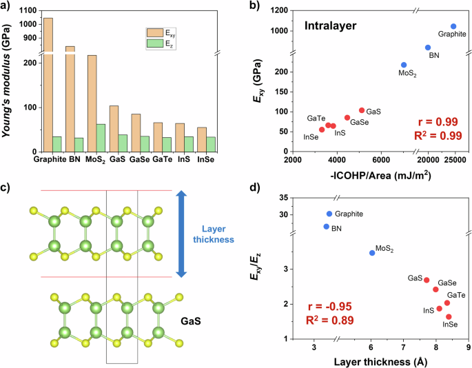
a Elastic modulus for typical hexagonal vdW crystals, Exy and Ez are the in-plane and out-of-plane elastic modulus, respectively. b Exy versus total -ICOHP per unit area for the cross-layer plane. c Schematics of monolayer thickness for GaS. d Exy/Ez ratio versus monolayer thickness (tl). r and R2 are the Pearson correlation coefficient and the linearity coefficient, respectively.
It is interesting to scrutinize the Exy/Ez ratio and treat it as a descriptor of the anisotropy. As shown in Fig. 4d, the Exy/Ez ratio varies with materials, but a clear decreasing trend is seen between this ratio and the layer thickness (r = −0.95). This phenomenon can be attributed to chemical bond origins. As the tl becomes larger, the electron density of intralayer cation-anion bonds decreases overall. In contrast, the electron density of the interlayer interactions remains at a relatively low level, with no huge changes in absolute values. Consequently, the difference between interlayer and intralayer bonding strength decreases, in other words, the anisotropy of materials decreases.
Modulation of mechanical properties by superlattice structure
The peculiar structure of vdW materials provides a large room for structure modulation and property tuning. Typically, the superlattice design has been found to be an effective way to modulate the physical properties and expand the applications of vdW materials in photoluminescence53, electrocatalysis54, and energy storage55. Here in this section, we explore the feasibility of building superlattices to modulate the chemical bonds and the mechanical properties. We constructed the superlattice of IIIA-VIA group compounds (GaS/GaSe and GaTe/InSe, see Fig. S6) for calculations. The superlattices were constructed with two different matrix materials stacking layer by layer alternately, and the lattice mismatch was less than 6%. As shown in Fig. 5a, the Ec,cross, and Eb,cross for the superlattice materials are well in the midst of the two parent materials, and the profile of GSFE curves is similar to other IIIA-VIA group compounds. Likewise, the in-plane modulus (Exy) also changes readily upon the introduction of the superlattice structure. By contrast, Ez for the superlattice materials does not change drastically since the interlayer interaction strength is quite close for these IIIA-VIA materials.
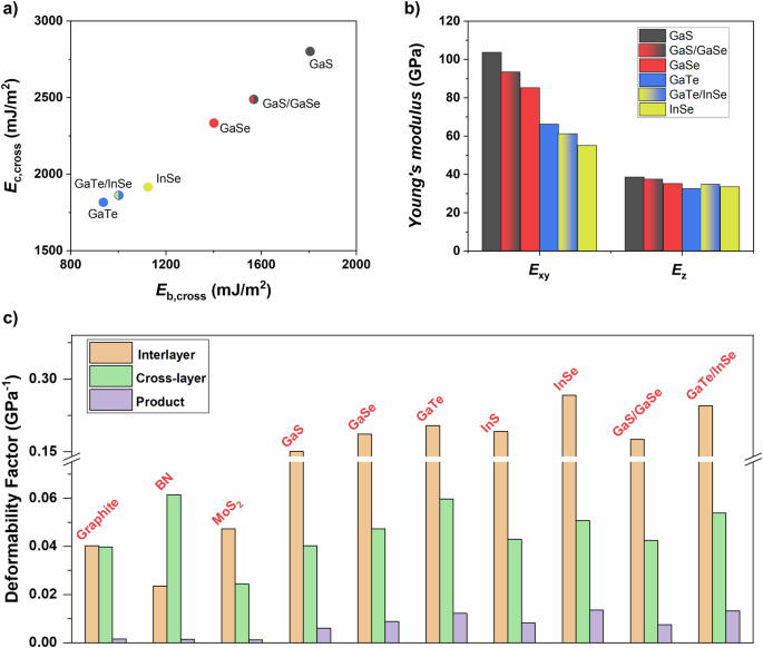
a Cross-layer cleavage energies, slip energy barriers. b Elastic modulus. c Interlayer, cross-layer deformability factor, and the product.
According to the above results, the deformation parameters of vdW crystals can be naturally classified into two types: one is highly correlated with an intralayer bond (in-plane modulus, cross-layer cleavage, and slip); the other depends more on the interlayer interactions (out-of-plane modulus, interlayer cleavage, and slip). The deformability factor Ξ(=left(frac{{E}_{text{c}}}{{E}_{text{b}}}right)left(frac{1}{{E}_{text{Y}}}right)) (the first term is the ratio of cleavage energy to slip energy barrier, and the second term is the reciprocal of the modulus along the slip direction) is useful to evaluate and screen potentially deformable materials19. Furthermore, we simply multiply the interlayer Ξ with the cross-layer Ξ, and the product is tentatively used to evaluate the overall deformability (purple columns). As shown in Fig. 5c, all the IIIA-VIA group compounds exhibit relatively high interlayer Ξ and product Ξ values as compared to graphite, BN, or MoS2. This indicates better deformability, basically related to the weaker, less covalent intralayer bonds alongside the multi-centered, diffusive interlayer interactions. The deformability factors of superlattice structures are generally between that of their matrix materials and also exhibit quite high levels.
In summary, by virtue of DFT calculations, we have investigated the correlation between the chemical bond features and the deformation parameters (slip barrier, cleavage energy, and modulus) of typical hexagonal vdW materials, including graphite, BN, TMDCs, and IIIA-VIA compounds. The intralayer bond strength can be well described by the corresponding -ICOHP while the interlayer interactions are too subtle to be fully captured. A generally positive correlation is seen between the bond strength and the deformation parameters. Noticeably, the cross-layer cleavage/slip energies and in-plane modulus are almost linear with the -ICOHP of intralayer bonds. Among these materials, the IIIA-VIA compounds, particularly InSe, are found to show the best deformability, which is basically decided by the weaker and less covalent intralayer bonds alongside the diffuse interlayer vdW interactions. By contrast, graphite and BN have the strongest intralayer bonds, while MoS2-like TMDCs show stronger interlayer interactions. Moreover, constructing the superlattice can effectively modulate the in-plane modulus and cross-layer slip behaviors. This work unravels bond-deformability correlation in 2D vdW crystals, being a useful guide to understanding and designing diverse deformable vdW materials for flexible, non-flat electronic, and energy devices.
Responses